Clear Sky Science · en
On the origin of bulk-related anisotropies in surface optical spectra
Why the shimmer of a surface matters
When light hits a polished semiconductor wafer, the reflected color and brightness carry subtle fingerprints of the atoms in the very topmost layer. Engineers routinely use this effect to monitor how device surfaces change during growth and processing. Yet for decades, a puzzling set of signals in these optical measurements looked as if they came from deep inside the material rather than from the surface itself. This paper shows that those “bulk-like” features can, in many cases, be traced back to the surface after all — once the role of electron–hole pairs and their localization is properly accounted for.

Looking at tiny differences in reflected light
The study centers on a technique called reflection anisotropy spectroscopy, which compares how strongly a surface reflects light polarized along two different in‑plane directions. Even tiny structural distortions in the outermost atomic layer can make the reflection slightly direction‑dependent, creating a sensitive probe of surface structure. However, many spectra show prominent peaks at energies known from bulk silicon, traditionally labeled as “surface‑induced bulk anisotropy” and often interpreted as coming from bulk‑like electronic states gently modified by the surface. This view has led some to argue that the method mainly sees the bulk and is therefore of limited use for surface science.
Following electron–hole pairs layer by layer
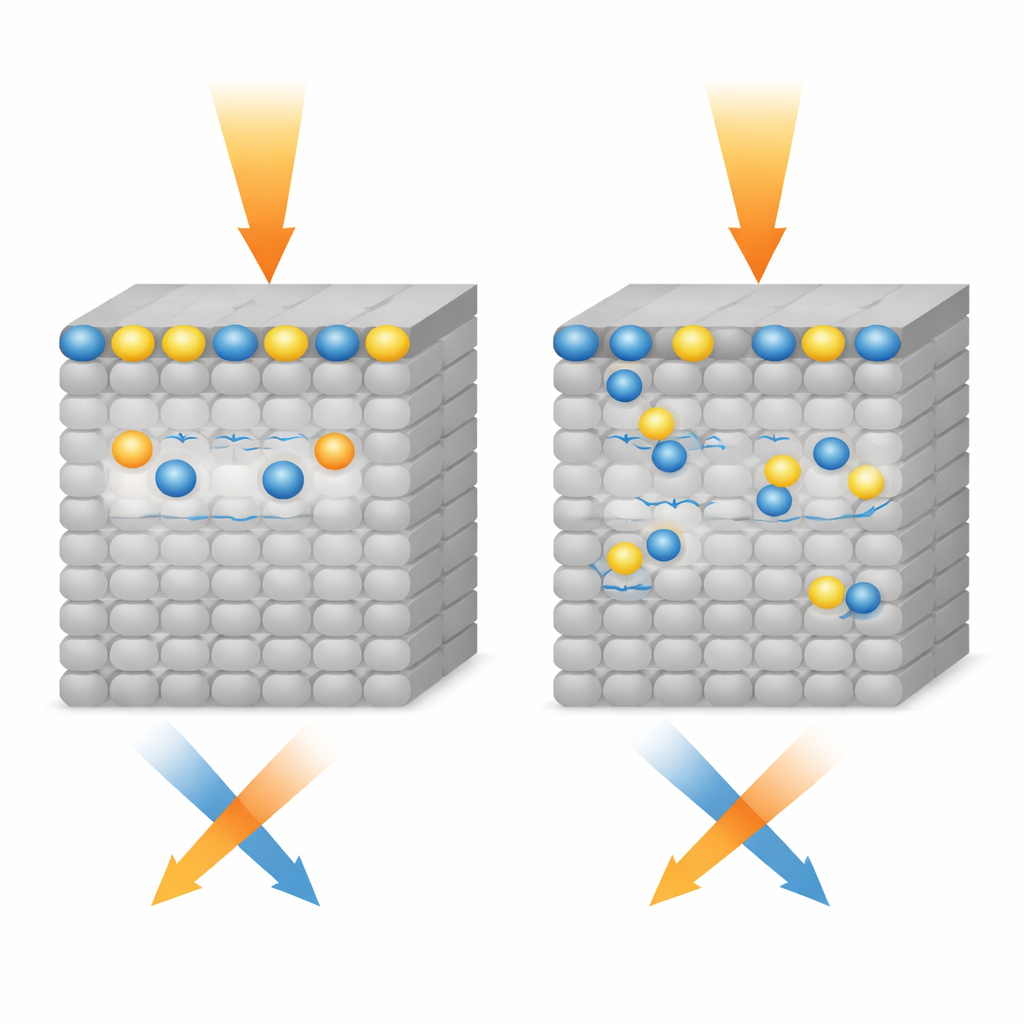
The authors revisit this long‑standing puzzle by taking excitons — bound pairs of excited electrons and the holes they leave behind — explicitly into account. Using state‑of‑the‑art many‑body simulations, they compute how excitons contribute to the direction‑dependent optical response of silicon surfaces coated with arsenic in different ways. Their key innovation is a new diagnostic, the layer‑resolved exciton localization measure. This tool evaluates for each exciton how much of its electron and hole wave function resides in each atomic layer of a model slab. In effect, it provides a map of whether an optical feature originates in the surface layer, in deeper subsurface layers, or in the interior of the crystal.
What really causes the “bulk-like” peaks
Applying this analysis to two arsenic‑modified Si(100) surfaces — one with symmetric arsenic dimers and one with a mixed arsenic–silicon–hydrogen pattern — the researchers find very different microscopic pictures hiding behind similar‑looking spectra. For the symmetric arsenic surface, most excitons that drive the strong spectral peaks near the well‑known bulk energies are sharply localized in the topmost layer. In other words, features that appear “bulk‑related” in energy are in fact dominated by surface states. On the mixed arsenic–silicon–hydrogen surface, excitons are more spread out through several layers, giving a more genuine mixture of surface and subsurface character, closer to the traditional surface‑perturbed bulk picture.
When the bulk boosts the surface signal
The team also shows with a simple model that the bulk material can strongly amplify or reshape purely surface‑driven anisotropies. Even if the bulk itself is perfectly symmetric, its ordinary optical response can modulate the surface contribution in such a way that peaks appear exactly at bulk critical energies. The authors call this effect bulk‑enhanced surface anisotropy. Together with cases where surface states just happen to lie at the same energies as bulk features, this mechanism explains how “bulk‑like” peaks can arise without being truly controlled by bulk electronic states.
What this means for reading surface spectra
By combining advanced exciton calculations with layer‑by‑layer localization maps, the work demonstrates that optical features at bulk‑characteristic energies do not automatically imply a bulk origin. Depending on the detailed surface reconstruction, they may stem from surface‑localized excitons, from more delocalized states, or from bulk‑enhanced modulation of surface signals. For experimentalists and technologists using reflection anisotropy to monitor semiconductor growth or prepare high‑quality silicon‑based devices, this means that careful, exciton‑aware interpretation is essential. The authors argue that neutral labels tied to energy, rather than generic “bulk‑related” tags, should be used unless a microscopic origin has been firmly established.
Citation: Großmann, M., Hanke, K.D., Bohlemann, C.Y. et al. On the origin of bulk-related anisotropies in surface optical spectra. Commun Mater 7, 83 (2026). https://doi.org/10.1038/s43246-026-01110-3
Keywords: reflection anisotropy spectroscopy, semiconductor surfaces, excitons, silicon optics, surface reconstruction