Clear Sky Science · en
In operando synthesis of an ultrathin dielectric based on crystalline gallium oxide
Why Shrinking Insulators Matters
From smartphones to data centers, every electronic device relies on thin insulating layers—called dielectrics—to keep signals under control. As engineers push components down to nearly atomic scales, these insulating layers must also become ultrathin without leaking current or breaking down. This paper reports a new way to grow a robust, atomically thin insulating layer made of gallium oxide directly on graphene, a wonder material already prized for its speed and strength. The work points toward future ultra‑compact, low‑power electronics built from carefully stacked two‑dimensional materials.
Building Tiny Layers Like a Sandwich
The researchers start with a carefully engineered sandwich of materials: a thick silicon carbide base, a single layer of graphene on top, and then a very thin film—only two to three layers—of a semiconductor called gallium selenide grown above the graphene. Each sheet in this stack is only atoms thick and interacts with its neighbors through gentle forces, making it easier to combine them without the structural problems that plague bulk materials. This carefully prepared structure provides the platform for turning the semiconductor layer into a new, ultrathin insulating film.
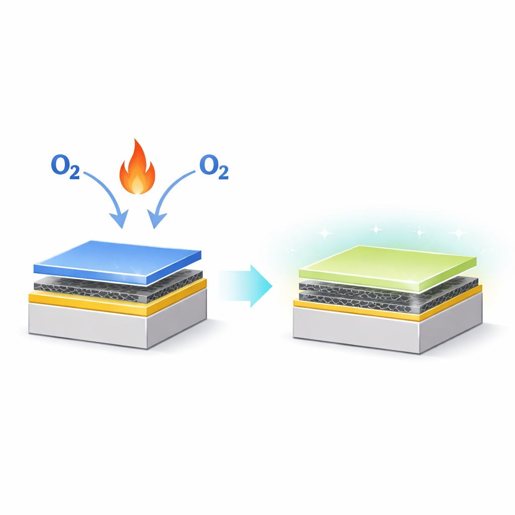
Turning a Semiconductor into an Insulator in Real Time
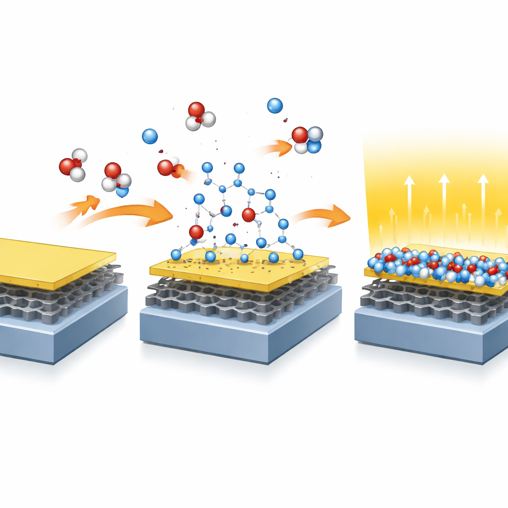
To convert gallium selenide into gallium oxide, the team heats the sample while exposing it to oxygen at controlled pressures. They monitor the change “in operando”—that is, as it happens—using a technique that detects how X‑rays knock electrons out of specific atoms. As the temperature rises above about 400 °C, selenium atoms begin to leave the surface while oxygen takes their place, gradually transforming the top layer into an oxide. Careful analysis of the signals from gallium, oxygen, carbon, and selenium shows that the resulting film has nearly the ideal chemical recipe for gallium oxide and that this conversion process can be reproduced reliably on different samples.
Seeing the Atomic Architecture
After oxidation, the team uses high‑resolution electron microscopes and surface probes to zoom in on the structure of the new film and its interface with graphene. Images reveal that the gallium oxide layer is about a nanometer thick—just a few atomic planes—and that it sits cleanly on the graphene with a very sharp boundary and an interlayer spacing of around 0.35 nanometers. Parts of the oxide are fully crystalline while others are partially ordered, but the graphene layer underneath largely retains its integrity for moderate oxidation conditions. Electron diffraction patterns confirm that long‑range order in the oxide is limited, yet local bonding remains well defined, enough to support a meaningful electronic band structure.
How the New Layer Behaves Electrically
The key test for any dielectric is how it handles electrons. Using angle‑resolved photoemission, the researchers map how electrons move in the graphene before and after oxidation. The distinctive “Dirac cone” pattern that defines graphene’s behavior remains essentially unchanged, showing that the new oxide does not disturb graphene’s fast‑moving electrons. At the same time, measurements of light‑induced currents and surface energy reveal that the oxide has a wide band gap of about 4.5 electron volts and large offsets relative to graphene’s energy levels. These large gaps and offsets make it difficult for electrons to tunnel through. Local measurements with a conductive atomic force microscope show that the oxide can withstand electric fields several times stronger than many conventional insulators before breaking down, even at thicknesses of only one to five nanometers.
What This Could Mean for Future Electronics
Together, these findings demonstrate a practical recipe for growing an ultrathin, high‑quality gallium oxide dielectric directly on graphene, without messy transfer steps or thick, disordered films. The process preserves graphene’s prized properties while adding a strong, stable insulating layer with excellent resistance to electrical breakdown. Because the method relies on chemically converting a starting semiconductor, it could be adapted to other two‑dimensional materials, offering a flexible toolbox of conducting and insulating layers for ultra‑scaled transistors, sensors, and even deep‑ultraviolet photonic devices. For the non‑specialist, the takeaway is that this work brings us closer to electronics where every functional layer is just a few atoms thick, yet still robust enough for real‑world technologies.
Citation: Rahman, K., Bradford, J., Alghamdi, S.A. et al. In operando synthesis of an ultrathin dielectric based on crystalline gallium oxide. Commun Mater 7, 78 (2026). https://doi.org/10.1038/s43246-026-01086-0
Keywords: gallium oxide, graphene, two-dimensional materials, nanoelectronics, dielectric films