Clear Sky Science · en
Ultrafast spatial hole burning of excitonic emission in monolayer WS2
Why tiny light waves in ultrathin materials matter
Engineers hope to build future information technologies not just with electrons, but with "excitons"—fleeting pairs of electrons and holes that carry energy as light inside a solid. This study looks at how these excitons move and disappear in a sheet of semiconductor only one atom thick. Understanding these ultrafast processes could lead to sharper sensors, faster light-based chips, and new ways to store and process information using light instead of electrical current.
A single-atom sheet under a laser spotlight
The researchers worked with monolayer WS2, a member of the family of atomically thin materials known as transition metal dichalcogenides. These materials are famous for binding light very strongly, forming tightly held excitons that dominate their optical behavior. The team peeled off ultrathin WS2 flakes, confirmed they were truly one layer thick, and then excited them with ultra-short laser pulses lasting less than a trillionth of a second. By recording how the emitted light changed in space, time, and color, they could watch excitons being created, diffusing outward, and fading away over tens of picoseconds (trillionths of a second).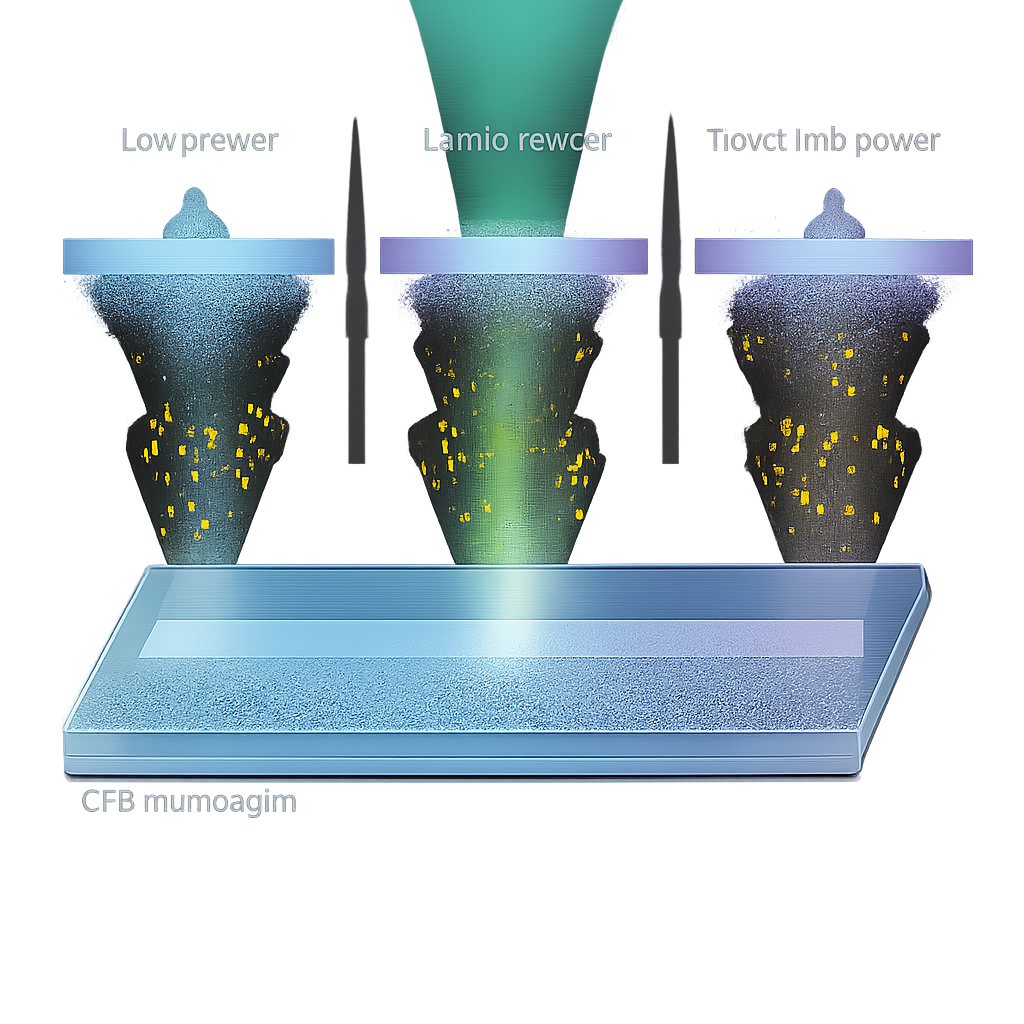
When the center goes dark instead of bright
At low laser power, the behavior looked simple: a bright spot of light appeared where the laser hit and gradually broadened as excitons diffused sideways, like dye spreading in water. But as the laser power increased, something counterintuitive happened. The very center of the illuminated region turned dark, while a bright ring formed around it—a pattern known as spatial hole burning or a "halo" profile. At even higher power, this central dark region re-brightened and eventually outshone the surrounding areas. Careful timing measurements showed that the light decayed faster when the hole appeared and then slowed again once the center brightened, hinting at a change in the underlying electronic environment rather than simple heating.
Local doping: how defects reshape the light
To uncover what was going on, the team compared light from the dark center with that from the bright outer ring in both time and color. They found that the outer region was dominated by emission from neutral excitons, while the dark center was dominated by charged excitons, or "trions," which emit more weakly and die out more quickly. This pointed to a spike in local doping—the effective number of mobile charges—in the center of the laser spot. The authors proposed a simple picture: under strong pumping, excitons frequently collide and annihilate each other in a process similar to an Auger reaction, freeing electrons and holes. The material naturally contains sulfur vacancies that love to trap holes and act like negative charge centers. As more holes are captured at these defects, the region becomes more heavily doped, neutral excitons are converted into trions, and the emission from the center is quenched, producing the observed dark hole.
Brightening again through light-driven chemistry
At still higher laser powers, the trend reverses and the center lights up again. Spectra taken below and above this threshold reveal that the brightened center is once more dominated by neutral excitons, meaning the material has been effectively "de-doped." The authors trace this to photo-oxidation: the intense laser assists oxygen- and water-related molecules in replacing sulfur atoms in the lattice. This light-driven chemistry changes how many free electrons are available, reducing the doping level and restoring efficient neutral exciton emission. Unlike the fast, reversible spatial hole burning, this oxidation involves rearranging atoms and turns out to be largely irreversible, matching what they observe when they lower the laser power again.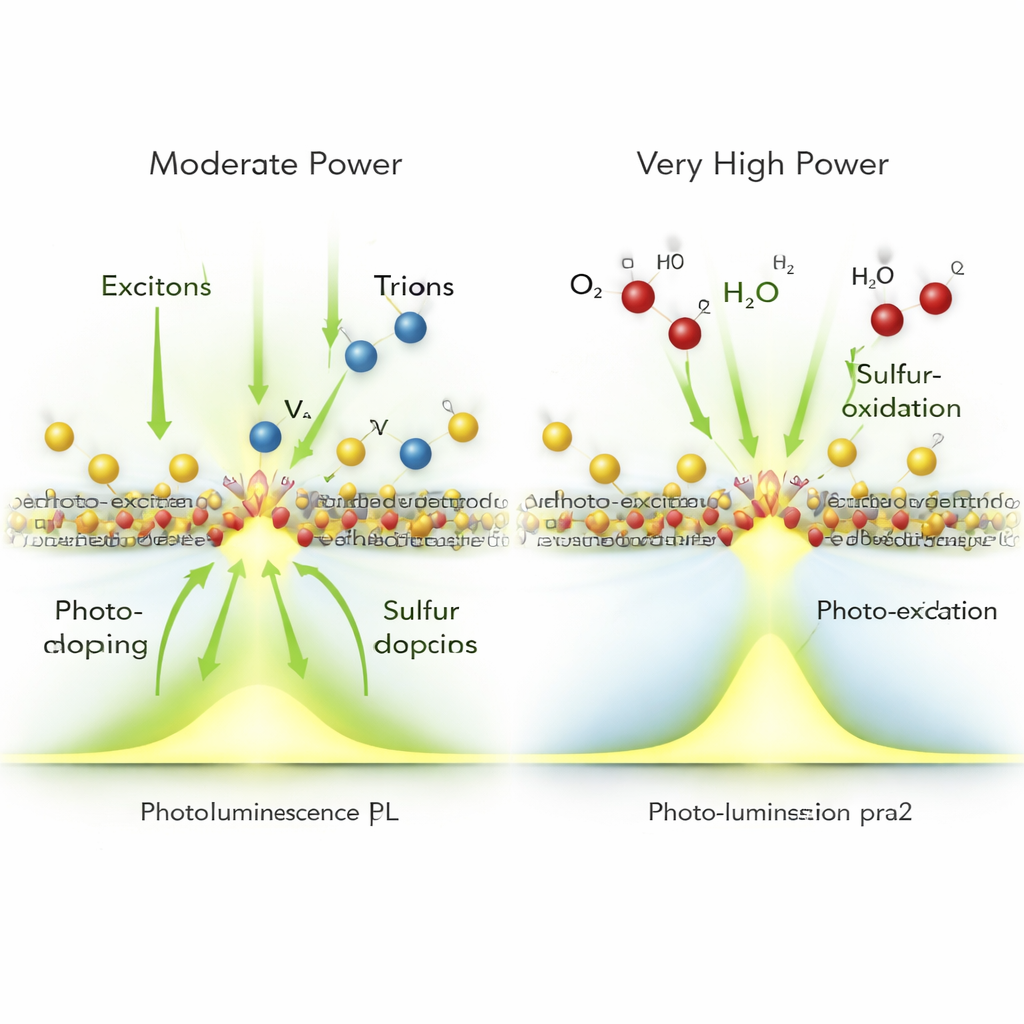
From complex physics to future exciton devices
To test their ideas, the team built a diffusion model that includes exciton-exciton annihilation, trapping of holes at sulfur vacancies, and laser-induced oxidation at high densities. The simulations reproduce both the sudden appearance of the emission hole and its later re-brightening, and closely match the measured light patterns in space and time. For non-experts, the takeaway is that a delicate balance between optical excitation, defects, and surface chemistry can strongly reshape how light moves and glows in atomically thin materials. By learning to control these effects, scientists move closer to building practical excitonic devices—circuits, sensors, and perhaps even computers—that run not just on electrons, but on the dance of light and matter bound together at the nanoscale.
Citation: Pan, Y., Zhu, L., Hu, Y. et al. Ultrafast spatial hole burning of excitonic emission in monolayer WS2. Commun Phys 9, 76 (2026). https://doi.org/10.1038/s42005-026-02516-8
Keywords: exciton transport, monolayer WS2, spatial hole burning, photo-doping, two-dimensional semiconductors