Clear Sky Science · en
Atomic-scale electrostatic engineering of flat bands in a K3P Lieb lattice
Building Quantum Highways for Electrons
Modern electronics largely relies on electrons zipping quickly through materials, but a very different world opens up when electrons are slowed almost to a standstill. In such “traffic-jam” conditions, their mutual repulsion and attraction dominate, giving rise to exotic states of matter like unconventional superconductors or electron crystals. This article reports a way to deliberately create and finely tune such slow-electron environments—known as flat bands—at the scale of individual atoms in an ultra-thin material made from potassium and phosphorus.
When Electrons Refuse to Move
In most solids, electrons occupy energy bands that curve smoothly with momentum, reflecting how easily they can move. A flat band is the opposite: the energy barely changes as the electron’s momentum varies, which means its effective mass becomes enormous and its motion is strongly suppressed. In this regime, even modest electrical interactions between electrons can dominate, potentially leading to unusual phases like superconductivity, fractional quantum Hall states, or “Wigner crystals” in which electrons arrange themselves in orderly patterns. Many research groups have tried to engineer flat bands using strong magnetic fields, complex layered structures, or finely twisted atomically thin sheets, but these approaches often require extreme conditions or difficult fabrication.
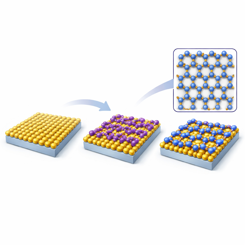
A Designer Atomic Lattice on Gold
The authors take a different route by building a specially patterned atomic lattice directly on a gold surface. They begin with a clean gold crystal and deposit phosphorus molecules onto it at high temperature, forming a well-ordered gold–phosphorus layer. Then they add potassium atoms and gently heat the system again. Under these conditions, the potassium atoms replace certain gold atoms, assembling themselves and the phosphorus into a new, ultra-thin compound called K3P. High-resolution scanning tunneling microscopy images reveal that the atoms arrange into a so‑called Lieb lattice—a repeating square pattern in which some sites are missing—stacked as a double atomic layer. This particular geometry is known from theory to favor flat electronic bands because electron waves interfere with one another in a way that cancels out motion along some paths.
Three Flat Bands and Their Hidden Players
To understand how electrons behave in this new lattice, the team combines direct tunneling spectroscopy measurements with detailed computer simulations based on quantum mechanics. They find three distinct energy regions in which the electrons form nearly flat bands. Two of these arise from quantum interference within the Lieb lattice itself, including subtle “next‑nearest” hopping between potassium atoms. The third flat band originates from potassium atoms sitting at the very top surface layer, whose electrons are strongly localized. Together, these three flat bands appear as sharp peaks in the local electronic density of states measured by the microscope—experimental fingerprints that closely match the theoretical predictions.
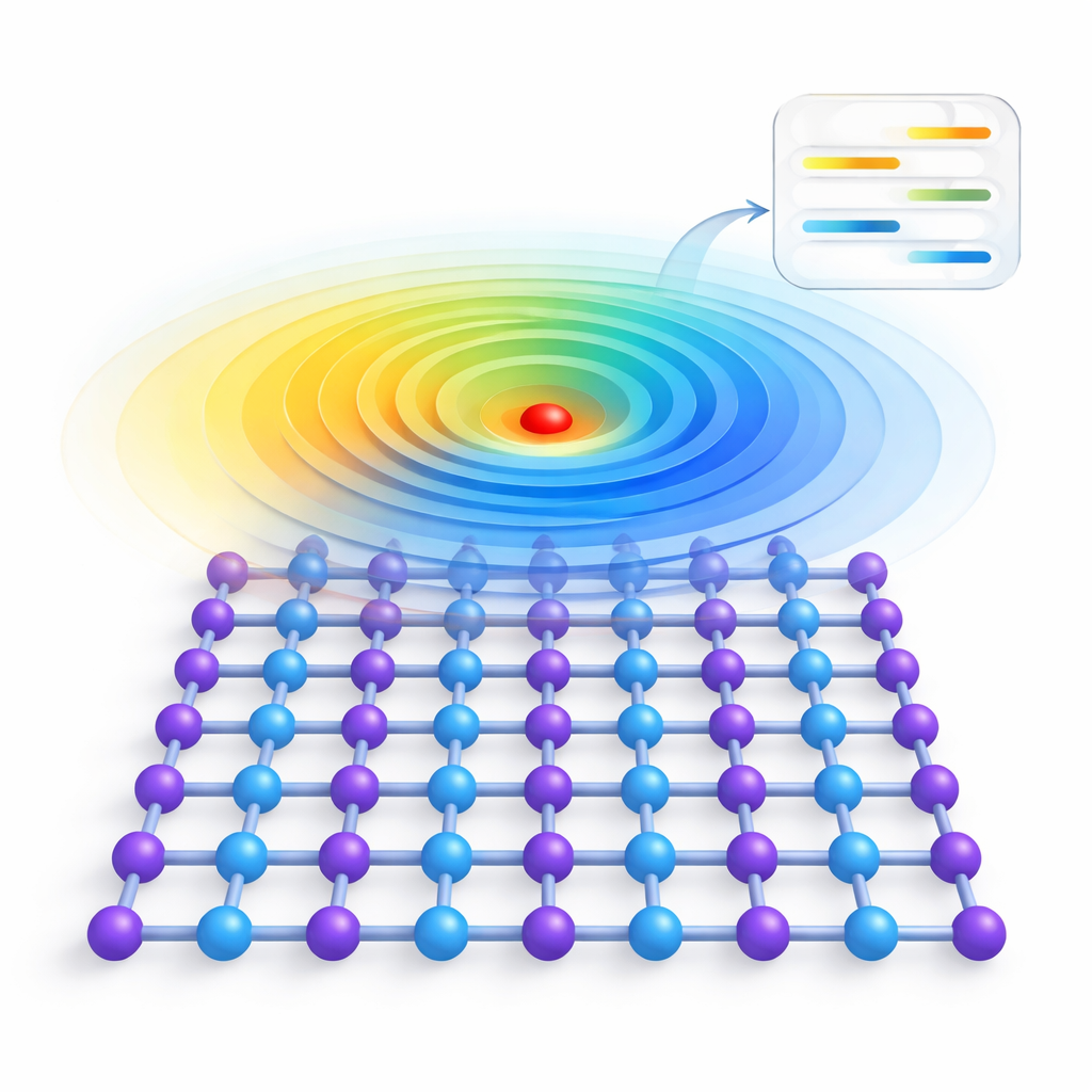
Using Atomic Defects as Tiny Electrostatic Knobs
Perhaps the most striking result comes from what would normally be considered imperfections: defects in the K3P layer. In the microscope images, certain defects show up as bright spots. By measuring how the electron energy levels shift as the probe is moved away from these spots, the researchers observe a smooth bending of the bands, just as if a tiny negative charge were placed at the defect site. The shift follows the familiar Coulomb law from basic electrostatics, meaning each defect behaves like a point charge embedded in the lattice. By mapping the electron signal over larger areas containing several such defects, the team directly images intricate contour patterns that match the equipotential lines predicted for multiple point charges. In effect, they demonstrate that native defects act as built‑in electrostatic knobs that can locally raise or lower the flat-band energies at length scales of just a few atoms.
Toward Programmable Quantum Materials
In everyday terms, this work shows how to carve an atomic “circuit board” in which the energy landscape experienced by slow, strongly interacting electrons can be shaped almost at will. The K3P Lieb lattice on gold forms a robust platform that hosts several flat bands, while its natural defects provide a precise way to tune these bands in space, much like adjusting the terrain in a miniature landscape to guide the flow of water. Looking ahead, the same scanning probe used to observe the system could be employed to intentionally create or move defects into designed patterns. That would turn this material into a programmable quantum simulator, where researchers could dial in specific electron arrangements or magnetic states and study how they emerge from the underlying, carefully sculpted flat-band landscape.
Citation: Li, Y., Liu, Y., Li, H. et al. Atomic-scale electrostatic engineering of flat bands in a K3P Lieb lattice. Commun Phys 9, 77 (2026). https://doi.org/10.1038/s42005-026-02512-y
Keywords: flat bands, Lieb lattice, scanning tunneling microscopy, 2D materials, quantum correlated states