Clear Sky Science · en
Charge transfer empties the flat band in 4Hb-TaS2, except at the surface
Why this strange superconductor matters
Most superconductors already bend our intuition by carrying electric current without resistance. The compound 4Hb–TaS2 goes a step further: experiments hint that its electrons may swirl in a chiral, or handed, pattern and break time‑reversal symmetry. To understand how such exotic superconductivity can arise, this study zooms in on how electrons are shared between different atomic layers inside the crystal and what that does to a special, almost flat electronic band that can strongly amplify interaction effects.
A crystal built from two very different layers
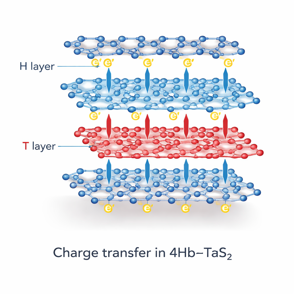
4Hb–TaS2 is a naturally layered material made from alternating stacks of two types of sheets, called H and T layers. The T layers develop a charge‑density wave pattern that groups 13 tantalum atoms into star‑shaped clusters, which in an isolated T sheet would host one electron in a very narrow “flat band.” Such flat bands often breed strong electron correlations, including Mott insulating behavior and even quantum spin‑liquid states, as discussed for the related 1T–TaS2 compound. By contrast, the H layers behave more like ordinary metals and are believed to host the superconducting electrons. The central question is whether the T layers in 4Hb–TaS2 still carry correlated electrons that could drive or shape its unusual superconductivity.
Probing the layers one tiny spot at a time
The authors used micro‑focused angle‑resolved photoemission spectroscopy (micro‑ARPES) to map how electrons occupy energy and momentum states, while resolving different surface terminations that appear after cleaving the crystal. Some surface patches expose a T layer; others expose an H layer, with additional T layers buried just below. By comparing these regions and supporting them with detailed quantum‑mechanical calculations, the team could distinguish the behavior of the topmost T layer, the subsurface T layer beneath an H sheet, and deeper, bulk‑like layers. This spatial selectivity is crucial because surface and bulk electronic structures can differ substantially.
Charge transfer that empties the flat band inside
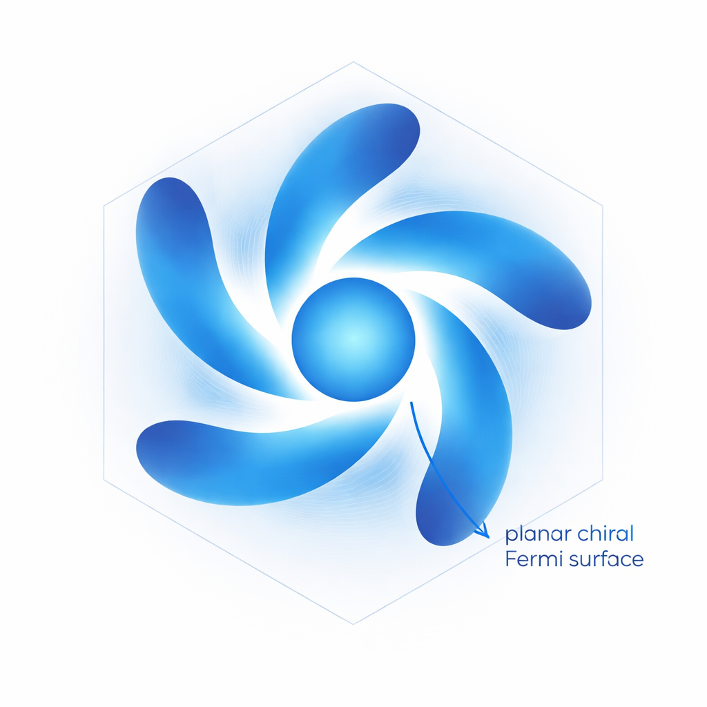
On surfaces where a T layer is directly exposed, the researchers found a metallic Fermi surface: a central pocket with petal‑like features forming a planar chiral pattern, meaning it lacks mirror symmetry in the plane. This indicates that the flat band in the surface T layer is only partially emptied; the team estimates about 0.2 electrons per 13‑atom cluster remain, implying that roughly 0.8 electrons have moved into the neighboring H layer. However, when they examined signals coming from a T layer buried beneath an H layer, they saw a very different picture. There, the characteristic T‑derived band was shifted to higher energy and showed no states at the Fermi level at all, indicating that the flat band is entirely emptied. Theoretical calculations for realistic 4‑layer stacks reproduced this energy offset between surface and subsurface T bands, confirming that charge transfer is weaker at the outermost surface but complete for T layers sandwiched between two H layers in the bulk.
No room left for strongly correlated electrons in the bulk
This full emptying of the flat band in bulk‑like T layers has major implications. It means that, inside the crystal, the T sheets are effectively band insulators because their potentially dangerous flat band has been vacated by charge transfer, not because electrons are frozen in place by strong mutual repulsion. As a result, theories that invoke local magnetic moments, Kondo‑like screening, or cluster Mott physics in the T layers to explain the unusual superconducting state no longer match the experimental reality of 4Hb–TaS2. The T surface can still host a lightly filled metallic flat band, which may help re‑interpret earlier tunneling experiments on engineered H–T bilayers, but this state is a surface feature rather than the engine of bulk superconductivity.
A layered superconductor linked by tunneling
For a non‑specialist, the key message is that electrons are strongly rearranged between layers in 4Hb–TaS2. The inner T layers donate essentially one electron per 13‑atom cluster to neighboring H layers, emptying their own flat band and becoming insulating spacers. Superconductivity then lives primarily in the metallic H sheets and must couple between them by Josephson‑like tunneling through these insulating T barriers, rather than through itinerant electrons in the T layers themselves. This revised picture narrows down the possible mechanisms behind the material’s chiral superconductivity and underscores how subtle interlayer charge transfer can completely reshape the behavior of quantum materials.
Citation: Date, M., Bae, H., Louat, A. et al. Charge transfer empties the flat band in 4Hb-TaS2, except at the surface. Commun Phys 9, 60 (2026). https://doi.org/10.1038/s42005-026-02498-7
Keywords: 4Hb-TaS2, charge transfer, flat bands, layered superconductors, angle-resolved photoemission