Clear Sky Science · en
Visualizing electronic structure of twisted bilayer MoTe2 in devices
Why twisting atom-thin crystals unlocks new physics
Modern electronics are built from crystals whose atoms sit in rigid, repeating patterns. But when scientists take two sheets just a few atoms thick and twist them slightly, the overlapping patterns form a larger, slow “beat” called a moiré pattern. This gentle twist can dramatically reshape how electrons move, giving rise to surprising behaviors such as superconductivity and unusual magnetic effects. In this work, researchers peer directly into the electronic structure of a twisted bilayer of molybdenum ditelluride (MoTe₂), a two-dimensional semiconductor, to understand why it hosts one of the most exotic states of matter discovered in recent years.
A new playground for strange quantum effects
Twisted “moiré” materials have emerged as a powerful platform for discovering novel quantum phenomena. One striking example is the fractional quantum anomalous Hall effect, where electrical conductance is locked to precise fractional values even without an applied magnetic field. This effect has recently been observed in twisted bilayer MoTe₂ with a twist angle of about four degrees. The underlying cause lies in the detailed electronic band structure—how electron energies depend on their motion inside the crystal. Until now, that structure had not been directly mapped in the actual devices where these effects appear, leaving theorists to make educated guesses.
Using light to read electron energies
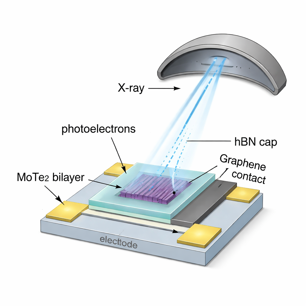
To see the band structure directly, the team used micro–angle-resolved photoemission spectroscopy (μ-ARPES), a technique that shines focused X-rays onto a sample and measures the energies and angles of emitted electrons. Because MoTe₂ rapidly degrades in air, the device was carefully assembled inside a glovebox and fully sealed between ultrathin sheets of hexagonal boron nitride (hBN). Unlike graphene caps used in earlier work, a monolayer of hBN is insulating, extremely thin, and transparent to outgoing electrons, allowing high-quality measurements while preserving the material’s intrinsic properties. By scanning the focused beam across the device, the researchers could selectively probe regions containing either a single MoTe₂ layer or the twisted bilayer.
Where the key electronic states live
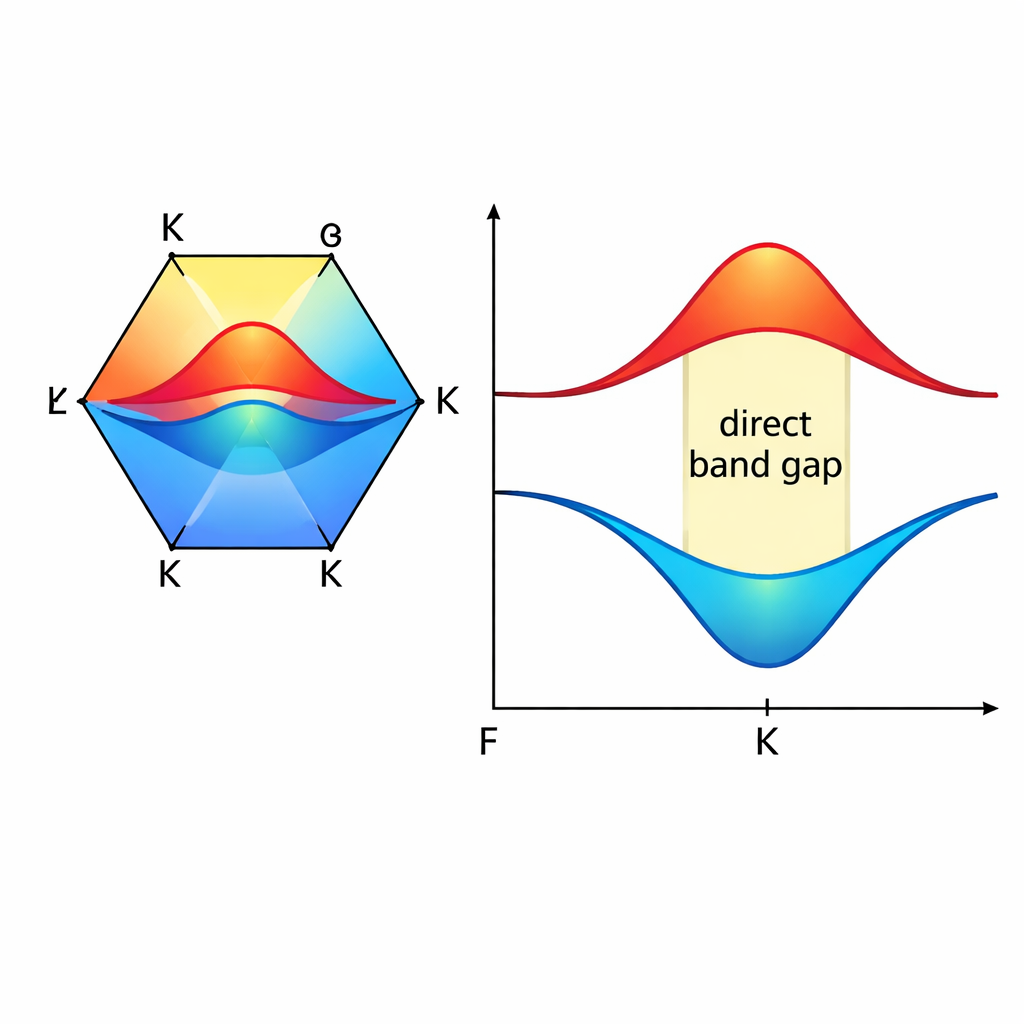
The μ-ARPES data reveal how twisting changes the energy landscape for electrons. In both the single layer and the twisted bilayer, the highest filled electronic states—the valence band maximum—sit at special points in momentum space called the K points, not at the crystal center (the Γ point). In the twisted bilayer, strong coupling between the two layers pushes the valence band near Γ upward, making it nearly as high in energy as the states at K, but still slightly lower. To find where the lowest empty states—the conduction band minimum—reside, the team gently added electrons by depositing alkali metal atoms onto the hBN surface. This shifted the Fermi level upward and brought the conduction band into view. Remarkably, in both the single layer and the twisted bilayer, the conduction band minimum also appears at the K point, revealing that twisted bilayer MoTe₂ has a direct band gap at K—unlike other similar moiré semiconductors, which typically have indirect gaps.
Checking theory and tuning the crystal
To interpret these findings, the researchers compared their measurements with detailed computer simulations based on density functional theory. The calculations correctly capture many trends, such as the rise of the valence band at Γ when two layers are stacked or twisted. However, standard calculations often predict that the lowest conduction states sit away from K at another point, labeled Q, in conflict with the experiments. The team explored how small in-plane strains—tiny stretches or compressions of the crystal—could shift these energies. They found that even about one percent biaxial strain can push the Q valley higher in energy than K, reconciling theory with observation and underscoring how sensitive the band structure is to subtle structural details such as strain, relaxation, and corrugation in the twisted lattice.
What this means for future quantum devices
By directly mapping where the crucial electronic states of twisted bilayer MoTe₂ reside and showing that it has a direct band gap at the same momentum point for both filled and empty states, this study establishes a solid foundation for understanding its unusual quantum phases. A direct gap at K is especially favorable for strong light–matter interactions and for the so-called “valley” physics thought to underlie the fractional quantum anomalous Hall effect. The work also demonstrates that high-resolution μ-ARPES can be performed on fragile, encapsulated devices and that their band structures can be tuned in place by controlled surface dosing. For non-specialists, the takeaway is that a carefully twisted, protected stack of atom-thin crystals can be engineered so that electrons organize themselves into new, highly correlated states, potentially enabling future low-power electronics and quantum technologies built from materials only a few atoms thick.
Citation: Chen, C., Holtzmann, W., Zhang, XW. et al. Visualizing electronic structure of twisted bilayer MoTe2 in devices. Commun Phys 9, 62 (2026). https://doi.org/10.1038/s42005-026-02497-8
Keywords: twisted bilayer MoTe2, moiré materials, direct band gap, angle-resolved photoemission, fractional quantum anomalous Hall effect