Clear Sky Science · en
Mapping diverse hysteresis dynamics in scaled MoS2 FETs using the universal method derived from TCAD modeling
Why tiny switches need reliable behavior
Modern electronics are racing toward ever-smaller transistors, and two-dimensional (2D) materials such as molybdenum disulfide (MoS2) are leading candidates for future chips. But as these switches shrink, their behavior can become inconsistent: the same device may respond differently depending on how it was used just moments before. This memory-like effect, called hysteresis, is often brushed aside as a minor nuisance. In this work, the authors show that hysteresis actually hides a wealth of information about the hidden flaws inside advanced transistors—and they introduce a universal way to read that information out.
How next-generation transistors are built
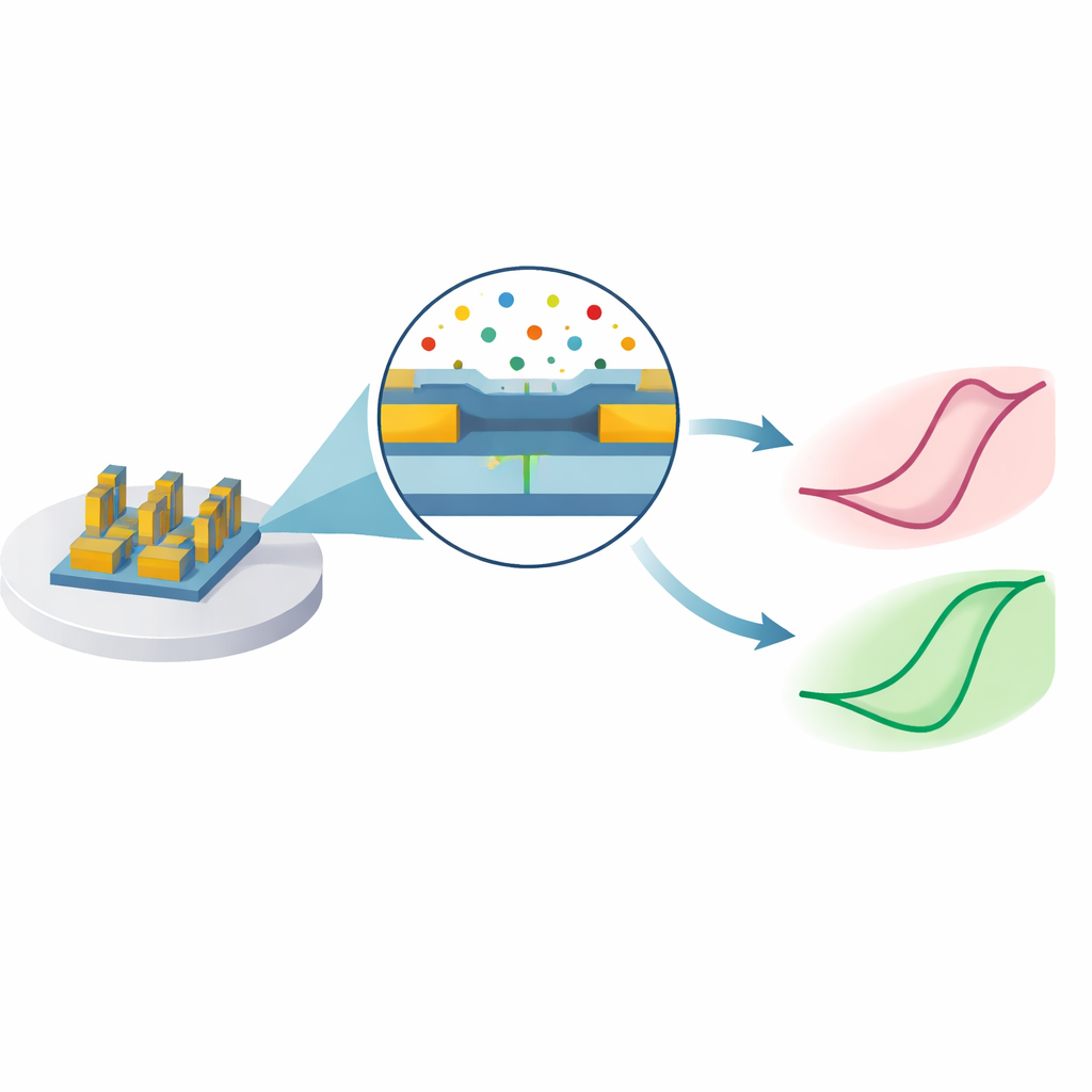
Future 2D field-effect transistors use an ultrathin MoS2 layer as the channel where current flows, covered by a very thin insulating oxide such as hafnium oxide (HfO2), and a metal gate on top. To keep shrinking devices, this oxide must be just about one nanometer thick in electrical terms, meaning that any individual defect inside it can strongly disturb the channel. These defects act as tiny traps that can temporarily hold or release electric charge. Because defects can reside at different depths inside the oxide and interact with both the channel and the gate, their collective behavior can either stabilize or destabilize the transistor in subtle ways. Understanding this defect landscape is crucial if 2D transistors are to compete with today’s silicon technology.
Why the transistor remembers its past
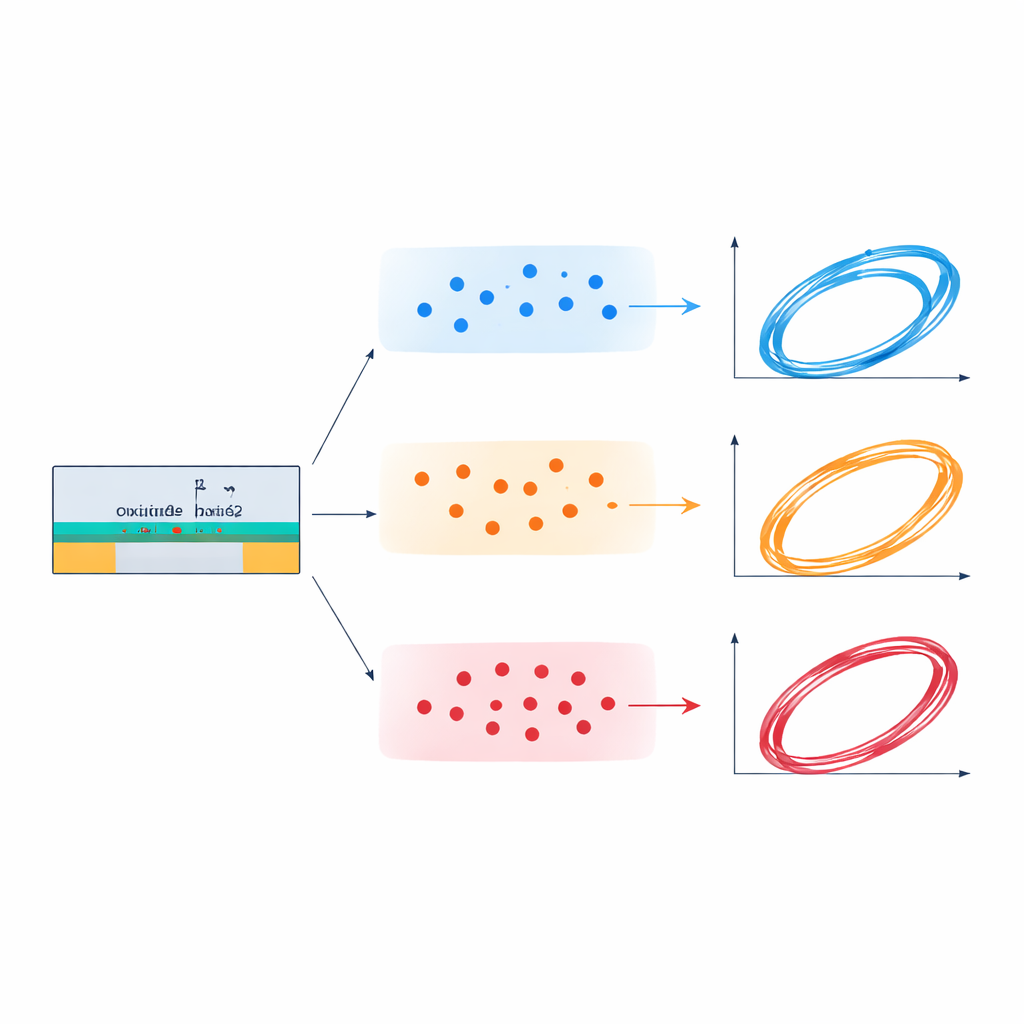
When engineers sweep the gate voltage up and down and record the current, they often find that the forward and backward sweeps do not coincide. This loop is the hysteresis. Traditionally, researchers measure the distance between the two curves at a single operating point and call that the hysteresis width, often concluding that it is “small” or “negligible.” The authors argue that this practice is misleading, especially for scaled devices in which different groups of defects may contribute in opposite ways. Depending on the measurement speed and operating current, the same transistor can show conventional clockwise loops, reversed counterclockwise loops, switching between the two, or even almost zero hysteresis when opposing effects cancel out.
A universal map hidden in the curves
To untangle this complexity, the team uses detailed computer simulations (TCAD) of nanoscale MoS2 transistors with carefully controlled defect populations at different depths in the oxide. They then propose a universal hysteresis mapping method. Instead of extracting a single number, they scan the hysteresis width across a wide range of currents—from slightly above the off state up to near the on state—and for sweep times spanning many orders of magnitude. This produces thousands of curves showing how hysteresis changes with measurement speed at each current. From these, they define upper and lower “universal hysteresis functions” that bound all possible behaviors. These envelopes cleanly reveal which kinds of defects are active, whether they interact mainly with the channel or with the top gate, and whether they favor clockwise or counterclockwise loops.
Linking fast loops to long-term drift
The same defects that cause hysteresis also drive slow drifts in transistor behavior under prolonged stress, a problem known as bias temperature instability (BTI). By simulating standard stress-and-recovery experiments, the authors connect features in their hysteresis maps to unusual BTI signatures, such as an apparent negative shift that only later relaxes toward a positive one. They show that traps near the channel tend to cause slow, mostly permanent shifts, while traps closer to the gate cause faster but largely reversible changes. Their method can be applied not only to simulated MoS2 devices but also to measured data from real MoS2 and WSe2 transistors made in research cleanrooms and pilot fabrication lines, including cases where drifting ions in the oxide join the charge-trapping game.
From complex data to practical guidance
By turning messy hysteresis loops into standardized maps, this work offers a powerful diagnostic for emerging transistor technologies. The method works directly on experimental datasets and does not require access to advanced simulation tools, making it broadly usable across labs. For engineers, the key message is that hysteresis is not just a flaw to be minimized, but a fingerprint of underlying reliability problems. Decoding that fingerprint with the proposed mapping method can guide better materials, cleaner interfaces, and smarter processing, helping 2D transistors progress from promising prototypes to truly dependable building blocks of future electronics.
Citation: Lv, Y.Z., Wu, Y.H., Cai, H.H. et al. Mapping diverse hysteresis dynamics in scaled MoS2 FETs using the universal method derived from TCAD modeling. npj 2D Mater Appl 10, 35 (2026). https://doi.org/10.1038/s41699-026-00671-8
Keywords: 2D transistors, hysteresis, oxide defects, device reliability, MoS2 FETs