Clear Sky Science · en
Hexagonal boron nitride: interlayer with atomic scale precision for interface engineering in functional materials and devices
Building Better Electronics with Invisible Spacers
Modern gadgets, from phones to quantum devices, depend on how well different materials touch and talk to each other. This review article explores a nearly invisible helper—atomically thin sheets of hexagonal boron nitride (hBN)—that sit between materials like a perfectly smooth, electrically controlled “spacer.” By changing just a few atomic layers of this spacer, engineers can dial up or dial down how strongly neighboring materials interact, opening paths to faster electronics, brighter light sources, and more reliable quantum technologies.
A Two-Dimensional Shock Absorber
Whenever two different materials meet, their boundary becomes a hot spot for new behavior: electrons can jump, waves can mix, and unwanted defects can appear. These interfacial effects are powerful but hard to tame because they depend sensitively on distance at the scale of individual atoms. Traditional insulating films tend to grow in patchy islands, with dangling bonds and defects that disturb nearby electrons. In contrast, hBN is a layered crystal that can be peeled or grown one atomic sheet at a time. Its surface is chemically quiet and atomically flat, so it forms clean, so-called van der Waals interfaces with many materials. By simply choosing how many hBN layers to insert, researchers can precisely set the separation between two crystals and thereby tune how strongly they influence each other. 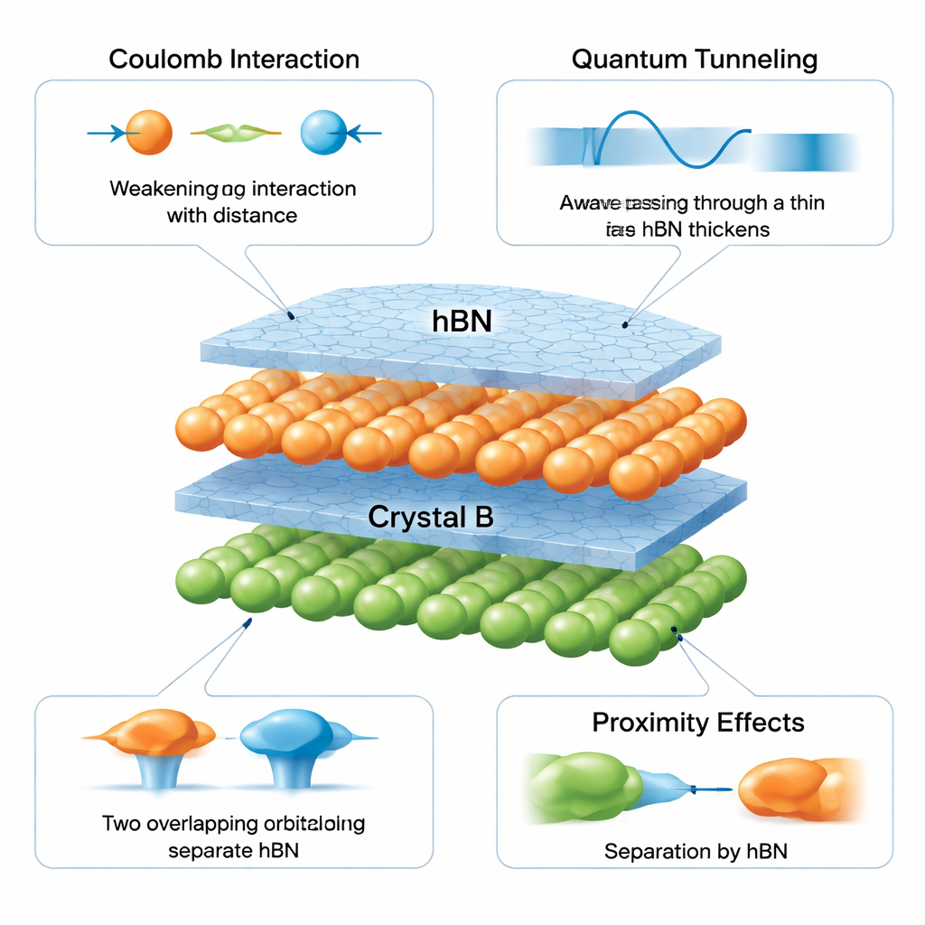
Tuning Charge Flow One Atomic Layer at a Time
In electronic devices, this atomic control becomes a powerful design knob. When dopant atoms are used to add charge carriers to a semiconductor, placing them too close causes the carriers to scatter and slow down; placing them too far away makes it hard to inject charge at all. An hBN spacer allows “remote doping,” where dopants sit behind a thin barrier. Experiments show that increasing the hBN thickness from about 1 to 2 nanometers cuts down scattering and boosts mobility, but also reduces the number of carriers, highlighting a delicate trade-off. At metal–semiconductor contacts, direct touching often creates troublesome electronic states that pin the energy levels and raise resistance. Inserting just two or three layers of hBN blocks this unwanted mixing while still allowing electrons to tunnel through, bringing the contact behavior closer to the ideal limit predicted in textbooks.
Light, Plasmons, and Atomic Spacers
The same thickness control matters when devices interact with light. In surface-enhanced Raman scattering, metal nanoparticles concentrate light into “hot spots” that can boost molecular signals by orders of magnitude, but direct contact between metal and molecules can cause chemical side reactions and confusing extra peaks. A thin hBN cap protects the molecules and metals while still letting them feel intense local fields. There is, again, an optimal thickness: if the hBN is too thin, chemistry spoils the spectrum; too thick, and the field at the surface weakens. Similarly, when atomically thin semiconductors such as transition-metal dichalcogenides are stacked with hBN in between, the spacer keeps neighboring layers from merging electronically while still allowing them to exchange energy efficiently. By picking the right hBN thickness, researchers can build multi-layer stacks whose light emission is even brighter than the sum of separate single layers.
From Lab Flakes to Wafer-Scale Films
To move from proof-of-concept devices to real technology, hBN spacers must be made reliably over large areas with atomic-level precision. The review surveys several growth techniques, including chemical vapor deposition, molecular beam epitaxy, and metal–organic vapor phase epitaxy. Each offers different strengths in purity, speed, and scalability, but all must solve the same challenges: controlling the exact number of layers, avoiding wrinkles caused by thermal stress, and minimizing defects that leak current. New strategies range from carefully tuning the solubility of boron and nitrogen in metal catalysts, to designing substrates that allow monolayer hBN to be grown in single-crystal form and then mechanically lifted off, and to using hydrogen plasma to relax wrinkles without chemicals.
Future Challenges and Opportunities
Despite rapid progress, fully exploiting hBN as an atomic-scale spacer will require better ways to see and control its imperfections and to integrate it cleanly with a variety of other materials. Many of the most sensitive imaging tools are slow and destructive, so researchers are developing indirect, non-destructive methods to map defects over large areas. At the same time, new growth and stacking methods—such as remote and van der Waals epitaxy—aim to build entire vertical device structures directly on hBN without messy transfers. The central message is that by mastering just a few layers of this simple crystal, scientists can program how materials interact at their boundaries, potentially reshaping the design of future electronic, photonic, and quantum devices.
Why This Matters for Everyday Technology
To a non-specialist, the idea that adding or removing a single atomic layer could change how a device behaves might sound extreme, but that is exactly what hBN interlayers enable. They act like ultra-thin, highly adjustable spacers that let engineers keep the “good” interactions—such as efficient charge or energy transfer—while suppressing the “bad” ones, like scattering, chemical damage, and leakage. If the current scientific challenges in growing and integrating hBN at scale can be solved, this material could become a standard building block for more efficient transistors, ultra-sensitive sensors, brighter displays, and robust quantum components, all tuned with atomic-scale precision. 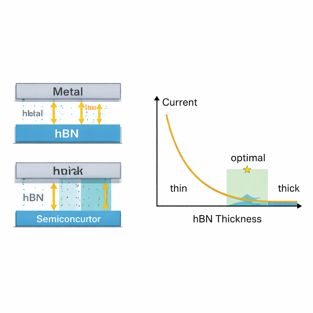
Citation: Jung, JH., Kim, CJ. Hexagonal boron nitride: interlayer with atomic scale precision for interface engineering in functional materials and devices. npj 2D Mater Appl 10, 28 (2026). https://doi.org/10.1038/s41699-026-00664-7
Keywords: hexagonal boron nitride, van der Waals heterostructures, 2D electronics, optoelectronics, interface engineering