Clear Sky Science · en
The two conduction bands of monolayer CrSBr on Au
Why this ultra-thin magnet matters
Electronics is steadily shrinking toward the scale of single atoms and layers only one atom thick. In that world, how a material touches a metal contact can completely change its behavior. This paper examines a promising ultra-thin magnetic semiconductor called CrSBr when it is placed on an extremely flat gold surface. The authors show that the metal contact does more than simply add or remove electrons: it actually changes the fundamental ways that electrons are allowed to move in the material.
Building a nearly perfect playground
To probe these effects, the researchers needed ultra-clean, ultra-flat conditions. They first grew a smooth gold film on a mica crystal and then “template stripped” it to reveal an almost atomically flat gold surface. Thin flakes of CrSBr were then peeled from a bulk crystal and pressed onto this gold in a protected environment. Using optical microscopes and atomic force microscopy, they identified regions that were just a single layer thick and others that were much thicker. The single-layer regions were large and smooth enough to study in detail with angle-resolved photoemission spectroscopy (ARPES), a technique that maps how electrons in a solid occupy energy and momentum states. 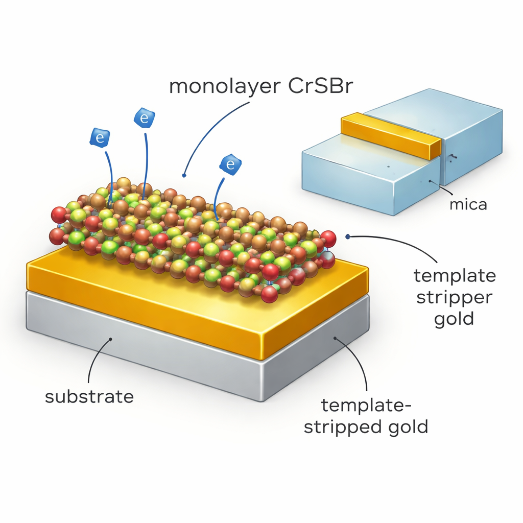
Watching the band gap shrink
In a semiconductor, the “band gap” is the energy window separating filled electron states from empty ones; it largely determines how the material conducts electricity and responds to light. In bulk CrSBr crystals, ARPES shows a sizeable band gap where no electronic states are occupied. But in the single-layer CrSBr on flat gold, electrons spill over from the metal into the CrSBr. This extra charge fills part of the material’s normally empty conduction band, allowing the researchers to see both the top of the valence band and the bottom of the conduction band directly. From this, they find that the band gap shrinks from roughly 2.0 electron volts in the bulk to about 1.3 electron volts in the monolayer on gold—a very large reduction. This means the metal contact and its electric screening can strongly tune CrSBr’s basic electronic properties.
Two electron highways instead of one
CrSBr is also interesting because its electrons and spins are highly directional. Theory predicts that a single layer should host two spin-polarized conduction bands—effectively two separate “highways” for electrons with different spins. Thanks to the charge transfer from gold, these conduction bands become occupied enough to be seen clearly in ARPES. The measurements reveal two distinct features: one band that curves strongly with momentum and another that is almost flat near the Fermi level, especially between key points (Γ and X) in the crystal’s momentum space. By analyzing constant-energy slices and energy spectra at specific momenta, the authors confirm that both bands contribute to the Fermi surface and estimate that the monolayer has gained about 0.05 extra electrons per chromium atom from the gold.
Breaking a hidden balance
In a free-standing monolayer of CrSBr, the atomic structure has a subtle “glide-mirror” symmetry that makes two chromium atoms in the unit cell equivalent. This symmetry normally forces the two conduction bands to meet, or be degenerate, at the edge of the Brillouin zone (the X point). Theory calculations reproduced this protected degeneracy. However, the ARPES data on CrSBr sitting on gold reveal a small but clear splitting between the two conduction bands at X. This tells us that the gold surface breaks the glide-mirror symmetry by making the two chromium sites feel slightly different environments. In other words, the metal contact does not just dope the material; it also lowers its symmetry and reshapes its band structure in a way that could affect transport and optical responses. 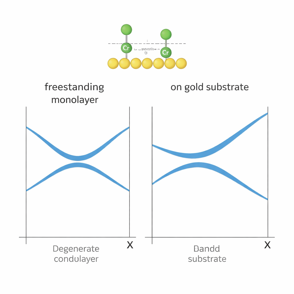
What it means for future devices
For a non-specialist, the takeaway is that contacts and substrates are not passive backdrops in ultra-thin electronics. In monolayer CrSBr on ultra-flat gold, the metal injects charge, squeezes the band gap, and even breaks a symmetry that once kept two electron paths locked together. These changes could influence how such materials behave in spin-based electronics, non-linear optical devices, and quantum technologies. The work shows that by carefully choosing and engineering the supporting surface, scientists can fundamentally reprogram the electronic landscape of atomically thin magnets.
Citation: Ghimirey, Y.P., Nagireddy, L., Cacho, C. et al. The two conduction bands of monolayer CrSBr on Au. npj 2D Mater Appl 10, 26 (2026). https://doi.org/10.1038/s41699-026-00662-9
Keywords: 2D magnets, CrSBr, gold interface, band structure, spintronics