Clear Sky Science · en
Fast interlayer energy transfer from the lower bandgap MoS2 to the higher bandgap WS2
Light Hopping Between Ultrathin Crystals
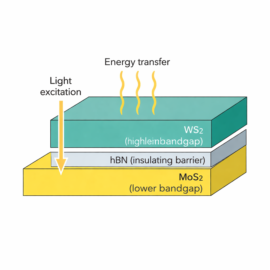
Turning light into useful energy inside electronics and solar cells depends on how quickly and efficiently that energy can move. This study explores an unusual kind of “light hopping” between two sheets of atom‑thin materials, where energy flows against the usual direction—from a lower‑energy material into a higher‑energy one. Understanding and controlling this unexpected route could help engineers design faster, more efficient optoelectronic devices built from stacks of 2D materials.
Stacking Atom-Thin Layers Like Lego Bricks
The researchers work with van der Waals heterostructures—stacks of atomically thin crystals that can be combined like Lego bricks. Here, they place a monolayer (single atomic sheet) of molybdenum disulfide (MoS2) beneath a monolayer of tungsten disulfide (WS2), separated by a very thin insulating spacer of hexagonal boron nitride (hBN). Normally, energy transfer—similar to the process used in photosynthesis—runs from a material with a higher energy gap to one with a lower energy gap. In this structure, however, MoS2 has the lower energy gap and WS2 the higher one. Yet the two have closely matched “excitonic” features—special light‑absorbing and light‑emitting states—so the team asks whether energy can flow in reverse, from MoS2 up into WS2, and how fast that process happens.
Watching Light Emission Change with Thickness
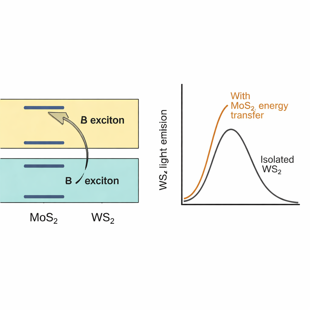
To track the energy flow, the scientists shine light on the MoS2 layer and monitor how brightly WS2 glows. They build several versions of the stack, keeping WS2 and the spacer the same but increasing the thickness of the MoS2 from one to several layers. This thickness change gradually converts MoS2 from a direct to an indirect energy gap material, which affects how easily excited electrons and holes stay in the “right” valley in momentum space to pass energy onward. Using photoluminescence excitation measurements—sweeping the laser color while watching WS2’s glow—they find that when MoS2 is a single layer, WS2 in the stack shines about three times brighter than an isolated WS2 sheet. As MoS2 gets thicker, this boost fades and eventually turns into a reduction in brightness, signaling that the special reverse energy transfer is strongest only when MoS2 remains a direct-gap monolayer.
Why the Energy Flow Fades in Thicker Layers
The team combines experiments with advanced computer calculations to explain this trend. In thicker MoS2, the favored electronic states shift so that excited carriers quickly fall into “side valleys” where they move less freely and are less likely to hop energy across to WS2. At low temperatures, vibrations in the lattice (phonons) are weaker, making it harder for carriers to climb back into the right states to transfer energy, and the enhancement of WS2 emission nearly disappears. At room temperature, stronger vibrations help shuffle carriers back, supporting energy transfer—but only efficiently when MoS2 is a single layer. Calculations of how strongly light couples to different excitonic states further show that the MoS2 “B” exciton and WS2 “A” exciton are both strong and nearly matched in energy, creating an especially favorable channel for this reverse flow.
Timing Ultrafast Energy Hops
To measure how quickly energy moves, the researchers use time‑resolved photoluminescence, firing ultrashort laser pulses and watching how the glow from each layer decays. They see that in the best‑matched monolayer stack, the overall lifetimes of the light‑emitting states do not simply get longer; instead, modeling of the full exciton dynamics is required. By combining these measurements with a detailed theory of dipole‑dipole (Förster‑type) coupling, they extract an energy transfer timescale of roughly 33 femtoseconds at room temperature—about thirty‑three millionths of a billionth of a second. This is faster than key competing processes inside MoS2, such as the reshuffling of carriers between different valleys, and is comparable to some of the fastest known charge transfer events in similar systems.
What This Means for Future Devices
In everyday terms, the study shows that when two ultrathin crystals with carefully matched light‑absorbing states are stacked with a nanoscale spacer, energy can leap uphill in energy extremely quickly, before it has time to get lost through other channels. This “reverse” energy transfer is highly sensitive to the thickness of one layer and to temperature, revealing how subtle changes in structure control the flow of energy. Such insights provide a blueprint for designing next‑generation light‑harvesting and light‑emitting devices in which energy is routed on demand across 2D material stacks, potentially enabling more efficient sensors, LEDs, and solar technologies built from atom‑thin building blocks.
Citation: Gayatri, Arfaoui, M., Das, D. et al. Fast interlayer energy transfer from the lower bandgap MoS2 to the higher bandgap WS2. npj 2D Mater Appl 10, 25 (2026). https://doi.org/10.1038/s41699-026-00661-w
Keywords: 2D materials, energy transfer, MoS2, WS2, optoelectronics