Clear Sky Science · en
Tunable surface electromagnetic waves at a graphene–hypercrystal boundary under magnetic bias
Guiding light along an invisible highway
Imagine being able to send ripples of light along a surface as tightly guided as a train on a rail, and to steer those ripples simply by turning a magnetic knob or adjusting an electrical dial. This study explores exactly such a possibility, using a single layer of graphene joined to an engineered "hypercrystal" material to create highly controllable waves of electromagnetic energy that travel along their shared boundary in the terahertz and mid‑infrared ranges—frequencies important for sensing, communications, and imaging.
A special boundary for surface waves
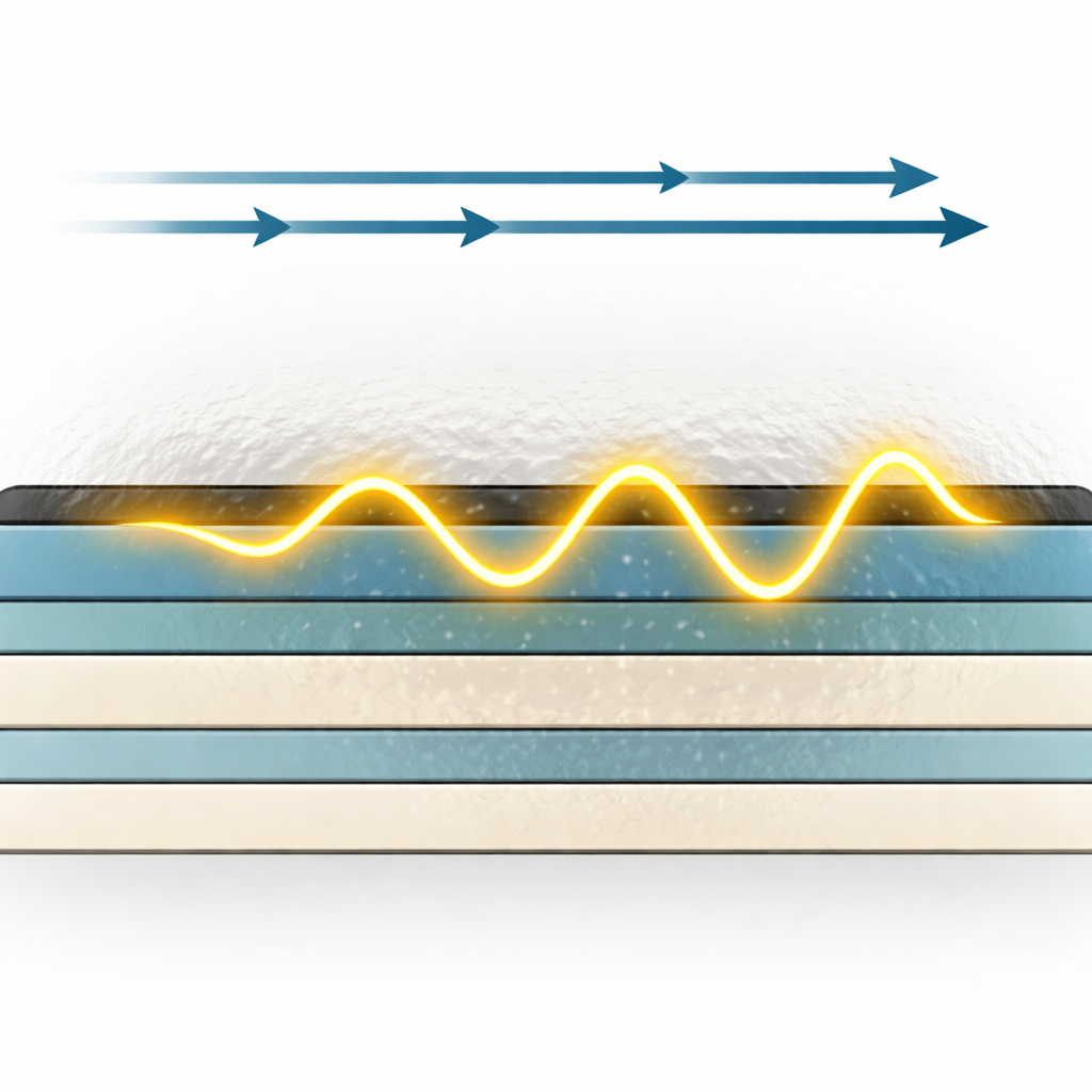
When light hits the boundary between two materials, it can sometimes become trapped and travel along that interface as a surface wave rather than spreading into space. These surface waves are prized because they confine electromagnetic energy to very small regions, amplifying interactions with matter. Graphene, a one‑atom‑thick sheet of carbon, is already known for supporting such tightly bound waves that can be tuned by changing its electrical properties. Separately, so‑called hypercrystals—layered stacks combining magnetic and semiconductor materials—can be designed to respond strongly to magnetic fields and to guide light in unusual ways. This work brings these two ideas together: a graphene sheet placed at the boundary between empty space and a magnetically responsive ferrite–semiconductor hypercrystal.
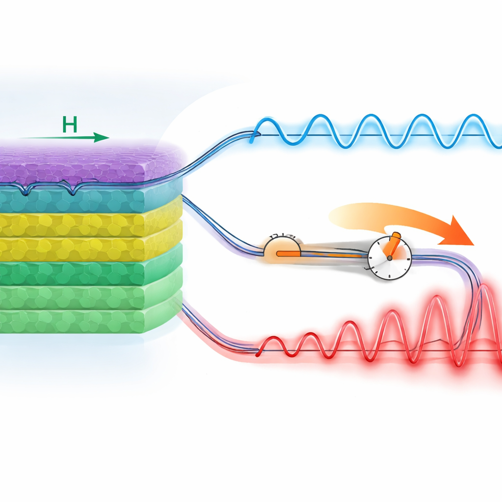
Building a magnetic, layered playground
The hypercrystal in this study is a carefully arranged sandwich of many ultra‑thin layers. One part of each repeating block contains a semiconductor and a simple dielectric (insulating) layer; another part contains a magnetic ferrite material and another dielectric. Repeating these blocks many times creates an effective medium whose overall response can be treated as if it were uniform but direction‑dependent: its electrical and magnetic properties differ along and across the layers. A static magnetic field is applied parallel to the graphene sheet, a configuration that strongly affects the ferrite and semiconductor layers but leaves graphene without the usual sideways (Hall) electrical effects. In this setup, graphene behaves mainly as a simple, tunable surface conductor along the interface.
Two kinds of surface ripples
Surface waves at this boundary come in two main flavors, depending on how their electric and magnetic fields are oriented. One type (TM) has its electric field largely normal to the interface and is strongly tied to how easily charges in graphene can move along the surface. The other type (TE) has its electric field lying along the interface and is instead governed mostly by how the layered hypercrystal responds magnetically. Using Maxwell’s equations together with an effective description of the stacked layers, the author derives analytical formulas that describe how each kind of wave travels and how quickly it fades away, explicitly showing how graphene’s conductivity and the hypercrystal’s anisotropy enter in different ways for the two polarizations.
How tuning graphene and magnetism reshapes the waves
With these formulas in hand, the study explores numerically how the surface waves behave as the external magnetic field and graphene’s chemical potential (a measure of its doping level) are varied. For TM waves, adding graphene significantly alters how fast the waves propagate along the surface and how tightly they are confined, shifting the range of magnetic fields over which they can exist and changing how strongly they are attenuated. Increasing graphene’s doping strengthens its influence: TM waves become more confined but also more lossy, and the magnetic‑field window in which they exist narrows. TE waves behave very differently. They appear only when the hypercrystal contains a sufficiently large fraction of magnetic (ferrite) material and are shaped almost entirely by the magnetic response of the layered structure. Changing graphene’s properties then produces only minor shifts in their cutoff points, propagation distance, and confinement.
What this means for future devices
Put in everyday terms, the graphene–hypercrystal boundary acts like a dual‑channel surface highway for light, where one lane (TM) can be actively controlled mainly by electrical tuning of graphene, while the other lane (TE) is opened and shaped mainly by the magnetic design of the hypercrystal itself. The work shows that by carefully designing the layered magnetic–semiconductor stack and then adjusting graphene’s doping and an external magnetic field, engineers can selectively tailor how different polarizations of surface waves propagate, how far they travel, and how tightly they hug the interface. This polarization‑selective tunability could underpin future compact sensors, switches, and reconfigurable photonic elements that operate in technologically important terahertz and mid‑infrared bands.
Citation: Fedorin, I. Tunable surface electromagnetic waves at a graphene–hypercrystal boundary under magnetic bias. Sci Rep 16, 8901 (2026). https://doi.org/10.1038/s41598-026-41299-4
Keywords: graphene surface waves, magnetoactive hypercrystals, terahertz photonics, tunable plasmonics, surface wave confinement