Clear Sky Science · en
Computational analysis of visible frequency plasmonic properties of graphene on wide band gap heterostructures
Why tiny light hotspots matter
Our phones, sensors, and future quantum gadgets all rely on pushing light into ever smaller spaces. When light is squeezed tightly, it can interact much more strongly with materials, boosting signals for detection and enabling faster, smaller optical components. This article explores how a single sheet of carbon atoms—graphene—sitting on top of another ultra-thin material can concentrate visible light into nanoscale hotspots at its edges, and how simply changing the underlying support layer can turn this effect on or off like a switch. 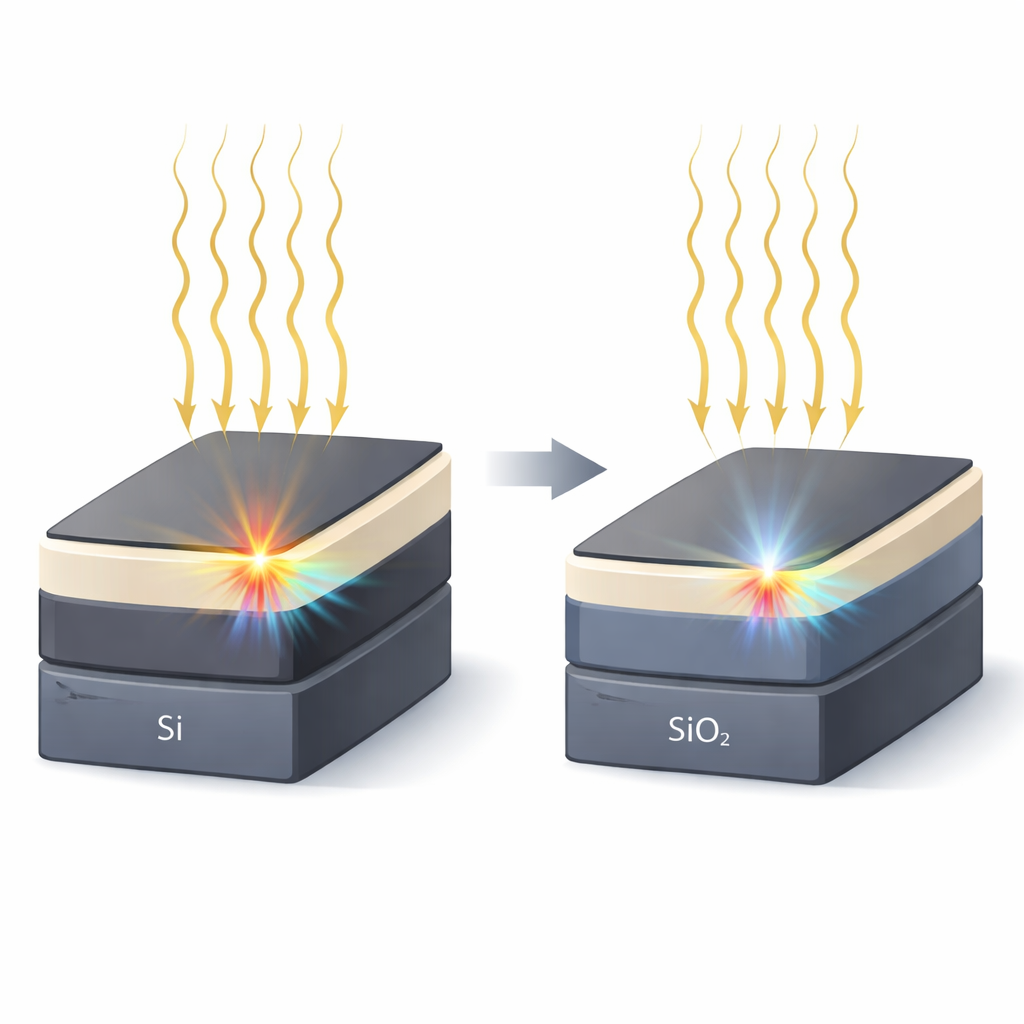
Building a layered playground for light
The researchers focus on a carefully stacked structure: a thin film of graphene draped over a flake of hexagonal boron nitride (h-BN), itself resting on a silicon chip or on a silicon chip coated with silicon dioxide (SiO₂). Graphene behaves like an extremely thin conductor, while h-BN is an excellent electrical insulator that also shapes the geometry of the edge where the flake ends. Instead of fabricating many samples, the team uses advanced computer simulations to calculate how electromagnetic fields behave in and around these layers when they are illuminated with visible light of specific colors, similar to those used in common red and green lasers.
Finding the sweet spot at the edge
The simulations reveal that the edges of the graphene/h-BN flake are special. When the stack sits directly on silicon, the electric field—the quantity that tells us how strongly light interacts with the material—can become up to ten times stronger at the edge than on a flat graphene-on-silicon surface without h-BN. This intense concentration depends sensitively on how thick both graphene and h-BN are. The effect appears for graphene from about a single layer up to several layers thick, but is strongest when the h-BN flake is in an intermediate thickness range of roughly 80–100 nanometers. At this “just right” thickness, the simulated field lines bunch up and point nearly straight across the edge, a configuration that is known to greatly amplify Raman scattering, a light-scattering signal widely used to read out material properties. 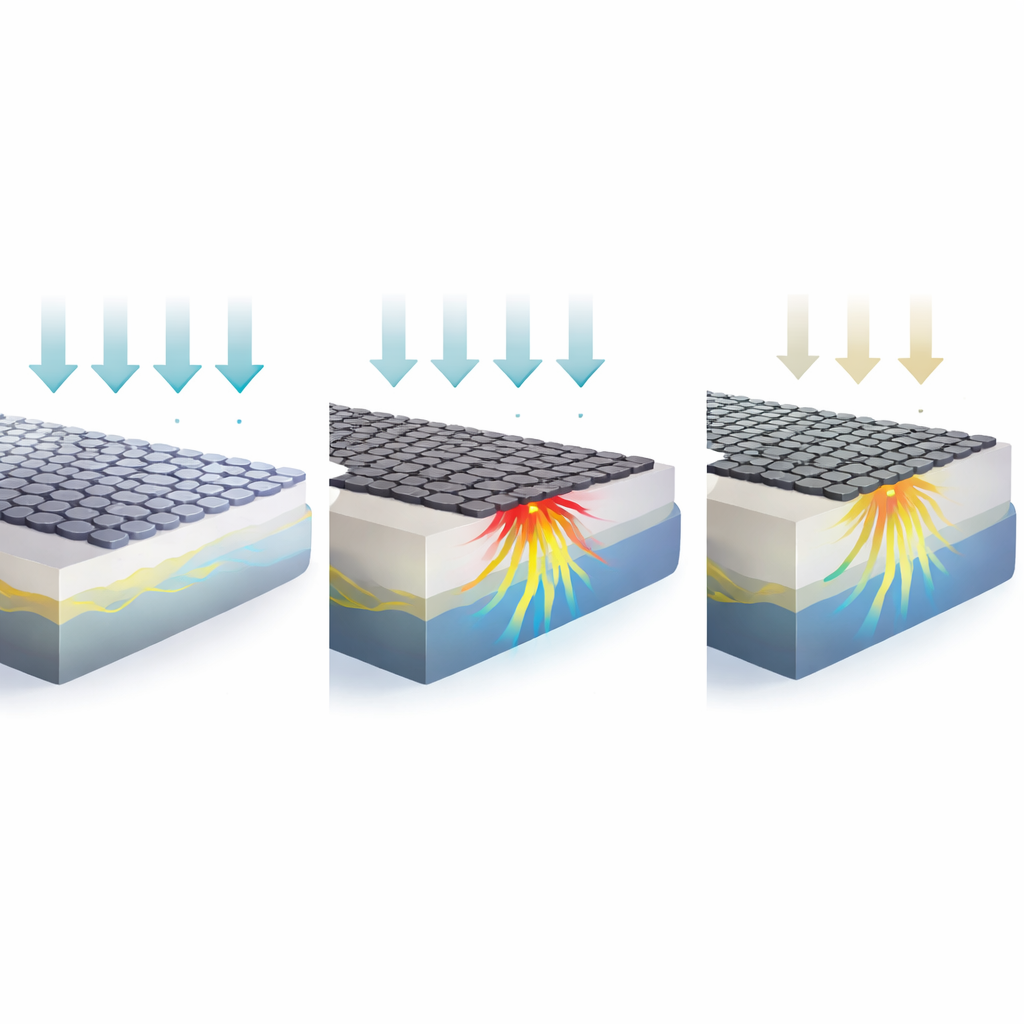
When the support layer shuts the hotspot off
The story changes dramatically when a silicon dioxide layer is placed between the silicon chip and the h-BN flake. Under otherwise similar conditions, the simulations show that the electric field near the graphene edges becomes much weaker and loses its tightly focused character. The strength of the field is now lower than for a simple flat graphene-on-SiO₂ reference, and changing the graphene thickness barely helps. Varying the h-BN thickness on SiO₂ produces only modest and very different patterns of field concentration. These findings match earlier experiments in which the Raman signal was strongly enhanced at edges on bare silicon but noticeably suppressed when the same kind of graphene/h-BN flake sat on SiO₂. Together, the results highlight that the conductivity of the underlying substrate—silicon versus insulating SiO₂—plays a crucial role in feeding charge into graphene to support these visible-light hotspots.
Probing the color and shape of the hotspots
Beyond a single laser color, the authors sweep through a range of visible wavelengths in their simulations. They predict that the most dramatic edge enhancement should occur for green to blue-green light, suggesting new experimental tests with shorter-wavelength lasers. They also build a full three-dimensional model, confirming that the edge hotspot remains highly localized along the step where the h-BN flake ends, and that its exact shape depends on the polarization—or direction—of the incoming light waves. Finally, the researchers show that the same basic principle can work with other wide-bandgap materials, such as diamond and alumina (Al₂O₃), pointing toward chip-friendly designs that go beyond a single choice of insulator.
From theory to future devices
In everyday terms, this work explains why certain combinations of ultrathin layers and substrates act like powerful “light funnels” at their edges, while others do not. By mapping out how edge intensity changes with layer thickness, material choice, and light color, the study offers a design toolkit for engineers who want to boost optical signals without resorting to traditional metals. Such controllable nanoscale hotspots could improve chemical and biological sensors, on-chip optical links, and future quantum technologies. In short, the article shows that with the right stacking of atomically thin materials on a suitable support, it is possible to tune where and how strongly light concentrates, using theory to guide the next generation of graphene-based photonic devices.
Citation: Qamar, M., Abbas, G., Liao, M. et al. Computational analysis of visible frequency plasmonic properties of graphene on wide band gap heterostructures. Sci Rep 16, 9138 (2026). https://doi.org/10.1038/s41598-026-40039-y
Keywords: graphene plasmonics, heterostructures, nanophotonics, Raman enhancement, wide band gap materials