Clear Sky Science · en
Silvaco TCAD modeling, optical simulation, and optimization for high-current perovskite and u-CIGS tandem solar cells with efficiencies above 30%
Cleaner power from smarter sunlight harvesting
As the world looks for ways to cut carbon emissions while meeting rising energy demand, solar panels are under pressure to do more with every ray of sunlight. This study explores a new type of “tandem” solar cell that stacks two advanced light‑absorbing materials, aiming to squeeze more electricity out of the same sunshine while avoiding scarce or toxic elements like lead and indium. The work uses detailed computer simulations to show how such a design could realistically reach efficiencies above 30%, a major step beyond most panels on rooftops today.

Why stacking solar layers boosts performance
Conventional solar panels use a single light‑absorbing layer, which means they can only capture photons with enough energy to cross that material’s energy gap. Higher‑energy photons lose their excess energy as heat, and lower‑energy photons pass straight through, both representing wasted sunlight. A tandem solar cell tackles this by stacking two different absorbers. The top layer is tuned to grab the bluer, more energetic part of the spectrum, while the bottom layer is tuned to catch the redder, lower‑energy light that slips through. Because each layer works closer to its ideal energy range, the combined device can convert a larger share of sunlight into useful electricity.
Building a greener tandem: lead‑free and indium‑free
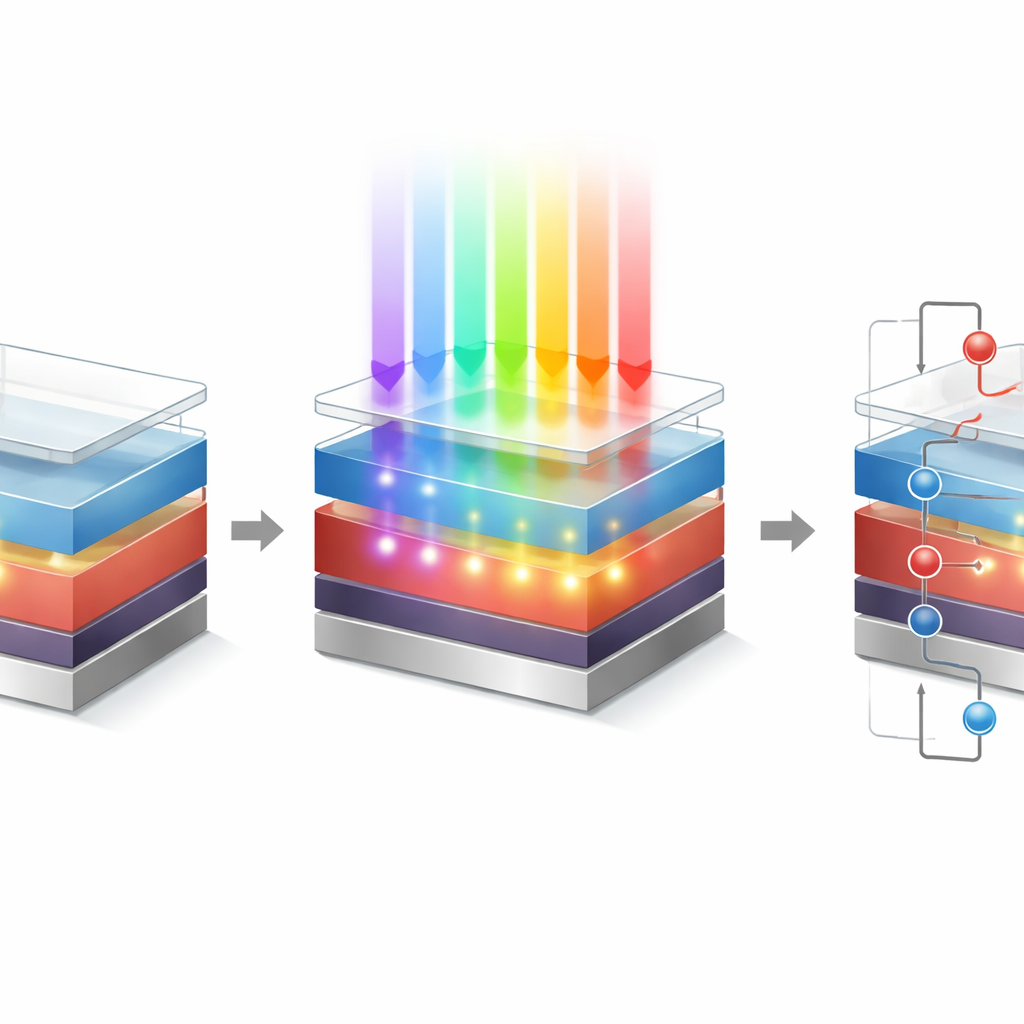
The authors design a two‑layer device in which the top cell is made of a lead‑free perovskite called methylammonium bismuth iodide (MBI), and the bottom cell is a thin film of the well‑known CIGS semiconductor (copper indium gallium selenide). To avoid the use of scarce indium in the transparent front electrode, they replace the widely used indium tin oxide (ITO) with fluorine‑doped tin oxide (FTO). FTO not only sidesteps supply concerns but also tolerates higher temperatures and mechanical wear, making it attractive for large‑scale manufacturing. The simulated single MBI cell with FTO reaches over 15% efficiency on its own, setting a solid foundation for stacking it with the CIGS layer underneath.
How careful tuning unlocks high efficiency
Simply piling one cell on top of another does not guarantee a better panel: both sub‑cells must deliver the same electrical current when wired in series, or the weaker one will limit the whole device. To solve this, the researchers use a two‑step numerical search to fine‑tune the thickness of the MBI layer so that the current from the top and bottom cells matches to within a tiny margin. They also model how light bounces, interferes, and is absorbed as it passes through every layer—from the glass cover and FTO front contact, through the perovskite and a very thin gold‑based connector, down into the CIGS film and metal back contact. At the same time, they calculate how electrons and holes move, recombine, and are collected, using physical models validated against real single‑cell experiments.
What the simulations reveal about the tandem cell
With these details in place, the simulated tandem device uses an MBI layer about 420 nanometers thick on top of a 500‑nanometer CIGS layer. The top cell soaks up nearly all light with wavelengths shorter than about 650 nanometers, while longer‑wavelength photons pass through and are efficiently captured by CIGS. The result is a shared current density close to 20 milliamps per square centimeter in both layers. Under idealized assumptions about material perfection and optical losses, the model produces a striking power conversion efficiency of roughly 36%. When the authors dial in more realistic levels of defects and interface losses, the performance settles to around 30%, still significantly above most commercial single‑junction panels and in line with the best tandem prototypes reported in recent years.
Why this approach matters for future solar panels
For non‑specialists, the key message is that smart design—rather than exotic new physics—can push solar panels well beyond today’s efficiency limits. By stacking a lead‑free perovskite tuned to blue light on top of a CIGS layer tuned to red light, and by replacing scarce indium with more robust FTO glass, the authors outline a path toward cleaner, more powerful, and more sustainable solar modules. Their simulations act as a roadmap, showing which layer thicknesses, contact materials, and interface qualities matter most. If materials scientists can approach these conditions in the lab and factory, solar panels that convert a third or more of incoming sunlight into electricity could become a practical reality, helping meet global energy needs with fewer panels, less land, and lower environmental impact.
Citation: Mosalanezhad, R., Shayesteh, M.R. & Pourahmadi, M. Silvaco TCAD modeling, optical simulation, and optimization for high-current perovskite and u-CIGS tandem solar cells with efficiencies above 30%. Sci Rep 16, 8611 (2026). https://doi.org/10.1038/s41598-026-39816-6
Keywords: tandem solar cells, perovskite photovoltaics, CIGS thin-film, lead-free solar materials, solar cell simulation