Clear Sky Science · en
Study on pore features in sintered die-attach microstructures based on machine learning
Why tiny pockets of emptiness matter
Modern power electronics, from electric cars to renewable energy converters, run hot and hard. Deep inside these devices, a thin bonding layer glues the semiconductor chip to its metal base and carries both heat and electricity. This layer is full of microscopic pores—tiny pockets of empty space—whose size, shape, and arrangement strongly affect how well the device works and how long it lasts. Yet engineers still debate which pore details really matter and how to read this hidden landscape from a few microscope images. This study tackles that problem by combining careful measurements with machine learning to uncover which pore features best describe the health of the bonding layer.

From hot-running chips to porous glue layers
Power modules based on new wide-bandgap semiconductors, such as silicon carbide, operate at higher temperatures and power levels than traditional electronics. Conventional solder joints can soften, creep, or crack under these conditions. A promising replacement is a joint made by sintering nano-sized copper particles at relatively low temperature. This process fuses particles into a sponge-like metallic layer shot through with pores. These pores influence strength, thermal conductivity, and long-term fatigue, and they can grow and link up into cracks during service. Because fully three-dimensional imaging is slow and expensive, engineers mostly rely on two-dimensional cross-sectional scanning electron microscope (SEM) images and a handful of simple indicators, such as overall porosity. The question is whether this limited view and a few basic measures are enough to judge the true structure.
Turning pore patterns into numbers
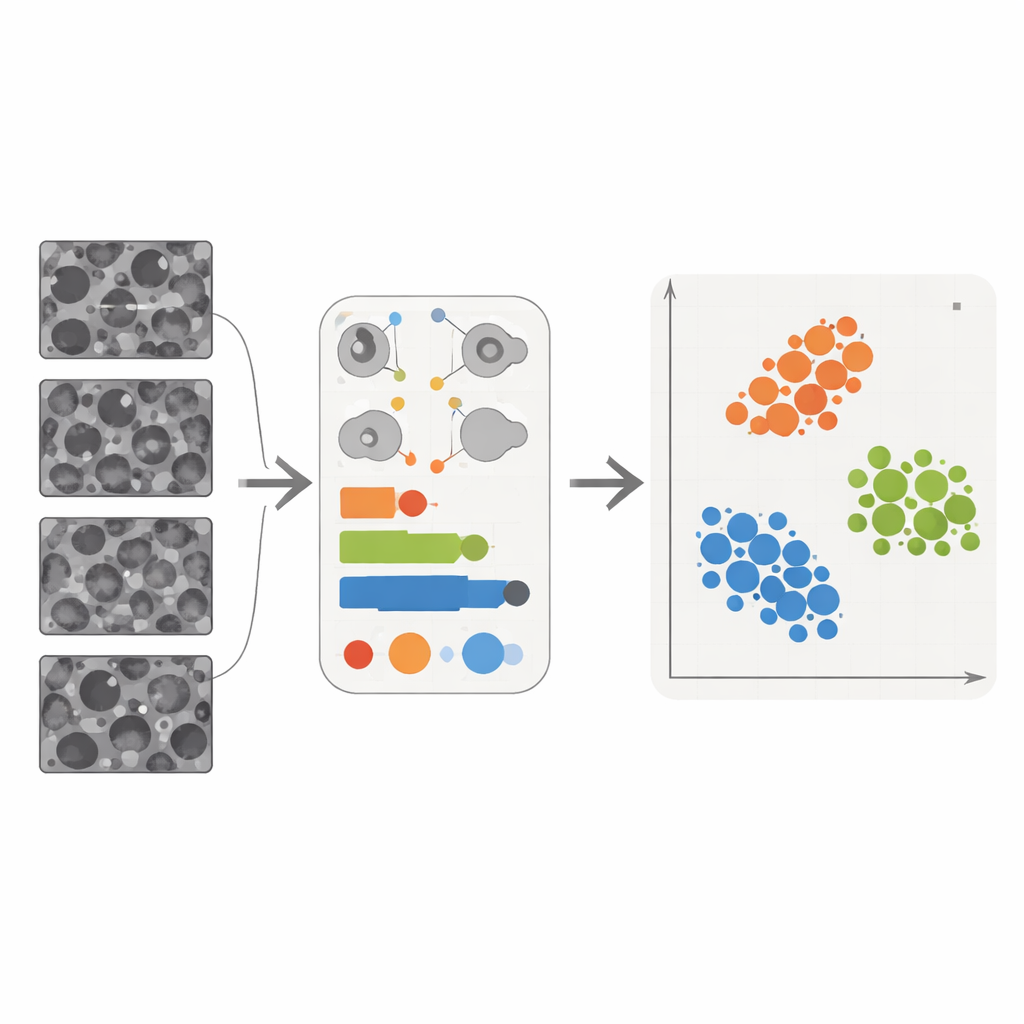
The researchers prepared copper sintered joints under four different combinations of temperature, pressure, and thermal cycling, then collected more than 120 high-magnification SEM images of their cross sections. Using image-analysis software, they automatically identified over one hundred thousand individual pores and quantified properties such as pore area, roundness, spacing to neighbors, and the length of the “necks” between nearby solid regions. From these pore-by-pore measurements, they built statistical descriptors for each image: how many pores it contained, how porous the region was, how tightly pores were packed, and how close their shapes were to neat circles. This created a rich numerical fingerprint of every small region in the joint.
Finding hidden order in messy data
Many of these numerical fingerprints turned out to be strongly related. For example, the more pores there were, the higher the porosity; the closer pores sat together, the shorter the necks between solid particles; and images with many nearly round pores also showed high average roundness. By analyzing these links mathematically, the authors showed that the features naturally fall into two families: one describing how pores are distributed in space and another describing their shapes. They then used a statistical technique called principal component analysis to compress each family into a single combined score: a “porosity factor” that summarizes how densely and evenly pores are arranged, and a “shape factor” that summarizes how regular their outlines are. Two simpler measures—typical pore size and typical aspect ratio—were kept as supporting descriptors.
Letting algorithms judge the microstructure
Armed with just these four descriptors, the team trained several different machine learning models to guess which processing condition each SEM image came from. Despite seeing only a small slice of the joint and only four numbers per image, the models correctly classified images more than 80 percent of the time, with a neural network reaching about 90 percent accuracy. When they compared this approach to an unsupervised deep-learning method that learned features directly from raw images, the physically meaningful descriptors actually performed better while remaining far easier to interpret. Further analysis showed that the combined porosity factor and shape factor contributed most to the models’ decisions, confirming that how many pores there are, how they are spaced, and how rounded they are carry the clearest imprint of the processing conditions.
What this means for better, longer-lasting devices
The study concludes that not every measurable detail in a micrograph is equally useful. Instead, a small set of thoughtfully chosen, physically grounded descriptors can capture most of the meaningful variation in sintered porous structures. For engineers, this means that a limited number of well-analyzed cross-sectional images can give a reliable picture of joint quality, even when the microstructure is uneven from place to place. These descriptors can also serve as inputs or targets for future predictive and generative models that design microstructures with desired strength or heat flow. In practical terms, the work offers a clearer, more efficient way to read the hidden pattern of pores that ultimately governs whether high-power electronics stay cool, strong, and reliable over years of demanding service.
Citation: Gao, R., Tatsumi, H., Kobatake, T. et al. Study on pore features in sintered die-attach microstructures based on machine learning. Sci Rep 16, 8803 (2026). https://doi.org/10.1038/s41598-026-39207-x
Keywords: sintered copper joints, pore microstructure, power electronics reliability, machine learning in materials, die-attach bonding