Clear Sky Science · en
Molecular dynamics simulation of atomic layer etching for sidewall damage recovery in GaN-based structures
Sharper, Brighter Chips for Future Screens
Modern gadgets—from virtual‑reality headsets to ultra‑high‑resolution displays—depend on ever‑smaller light sources made from gallium nitride (GaN). As engineers shrink these devices, the tiny sidewalls carved during manufacturing become badly scarred, wasting energy as heat instead of light. This paper explores a promising “nano‑polishing” method, called atomic layer etching, that could heal that damage atom by atom and pave the way for brighter, more efficient micro‑LEDs and power electronics.
Why Sidewall Scars Matter
GaN‑based devices are built from stacks of ultra‑thin layers, including InGaN/GaN multiple quantum wells that actually produce light. To separate millions of tiny pixels, manufacturers typically use a harsh dry‑etching step driven by chlorine‑based plasma. That process is fast and precise, but it bombards the exposed sidewalls with energetic ions, breaking bonds, mixing atoms, and leaving a thin, disordered “dead” layer. Conventional cleanup methods—gentle wet etches in chemicals like KOH or TMAH—remove only part of this damage and can’t reach deep into narrow, vertical walls. As devices keep shrinking, these scars become a major roadblock to performance and large‑scale production.
A Layer‑by‑Layer Atomic Scalpel
Atomic layer etching (ALE) aims to fix this by replacing the chaotic attack of plasma etching with a carefully choreographed, two‑step dance. First, a chemical step coats only the outermost atomic layer with chlorine. Next, a low‑energy argon ion beam knocks away that modified layer, much like planing off a single sheet of wood. Repeating this cycle can peel off damaged material with near‑atomic precision, while avoiding fresh harm. The authors used molecular dynamics simulations—a kind of virtual microscope that follows individual atoms in time—to test how well ALE could clean up GaN‑based sidewalls and which ion angles work best for both deep repair and smooth finishes. 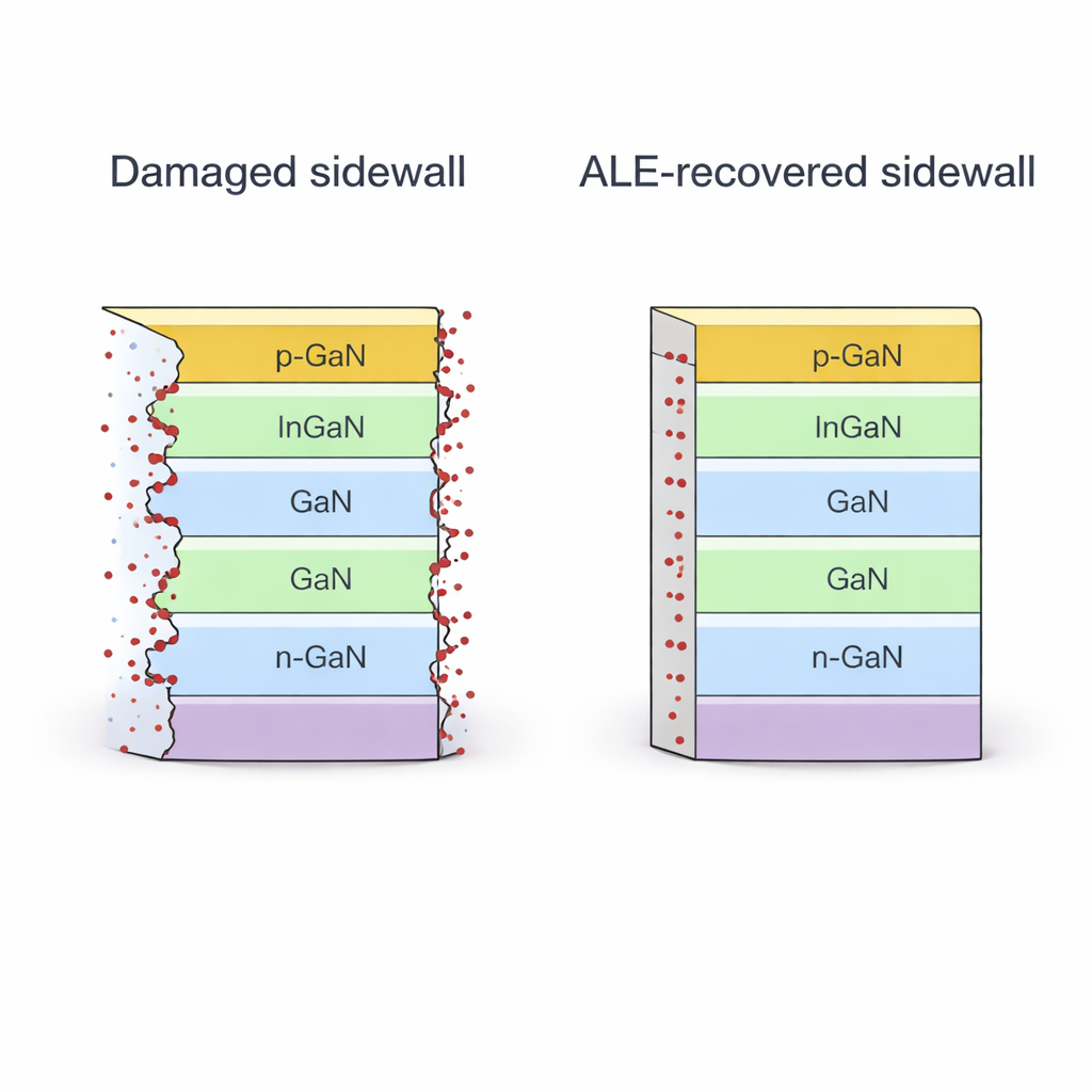
Simulating Damage and Healing Atom by Atom
In the simulations, the team first built ideal, defect‑free models of GaN, InGaN, and a realistic multi‑quantum‑well stack. They then “pre‑damaged” the sidewalls using virtual ion bombardment that mimics real plasma etching, creating three scenarios: high, medium, and low initial damage. After that, they applied repeated ALE cycles, changing the angle at which argon ions hit the wall—60°, 70°, or 80° measured from the surface. The simulations tracked how many atoms remained in a disordered state, how deep the damaged layer extended, and how rough the surface became as cycles progressed.
What Happens Inside the Layered Stack
The atomic‑scale movies revealed several key behaviors. The chlorine step reliably formed a thin, self‑limiting layer that was mostly removed in the next ion step, confirming the basic ALE mechanism. Interestingly, when shallow‑angle ions skimmed along the sidewall, some indium atoms from the InGaN wells migrated laterally into neighboring GaN layers. This subtle reshuffling made the surface composition more uniform across layers and helped the whole stack etch in a more even way. Across all three starting damage levels, ALE removed both surface and subsurface disordered regions, cutting the number of damaged atoms by more than about 47% and driving the remaining defect depth to similar, modest values. 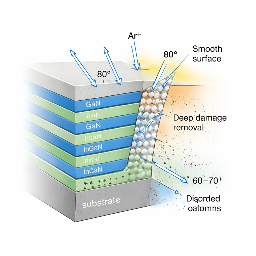
Finding the Sweet Spot for the Ion Beam
The angle of the ion beam turned out to be crucial. At lower angles (around 60°–70°), ions dug deeper and stripped away heavily damaged material more quickly, but left a somewhat rougher surface. At a steeper 80° angle, removal was slower and shallower, yet the resulting sidewall was notably smoother. This trade‑off led the authors to propose a practical two‑step recipe: first use 60°–70° incidence to clear out deep damage, then switch to about 80° for a final “polishing” pass that flattens the surface without over‑etching. Their simulations suggest that this dual‑angle approach works regardless of how badly the wall was damaged to begin with.
What It Means for Future Devices
To a lay reader, the bottom line is that the study shows we can, in principle, erase much of the invisible scarring left by harsh fabrication steps, one atomic layer at a time. By tuning the angle and energy of ion beams in atomic layer etching equipment, manufacturers could restore the crystal perfection of GaN‑based sidewalls, boosting light output and energy efficiency without sacrificing the small sizes demanded by next‑generation displays and power chips. The work also demonstrates how computer simulations can act as a design lab at the atomic scale, guiding real‑world process choices before a single wafer is etched.
Citation: Kim, E.K., Hong, J.W., Lim, W.S. et al. Molecular dynamics simulation of atomic layer etching for sidewall damage recovery in GaN-based structures. Sci Rep 16, 7110 (2026). https://doi.org/10.1038/s41598-026-38333-w
Keywords: atomic layer etching, GaN micro-LEDs, sidewall damage, molecular dynamics simulation, InGaN quantum wells