Clear Sky Science · en
Wafer-scale formation of MoS2 with controlled thickness and high uniformity via conversion of MoOx using H2S sulfurization and subsequent crystallization
Thinner, Smarter Electronics on the Horizon
Imagine phones, displays, and sensors built from sheets of material just a few atoms thick—lighter, more flexible, and more energy‑efficient than today’s silicon chips. One of the most promising of these ultrathin materials is molybdenum disulfide (MoS₂), but making it uniformly and reliably over entire silicon wafers has been a major roadblock. This paper reports a practical way to grow smooth, high‑quality MoS₂ films with tightly controlled thickness across full wafers, bringing next‑generation electronics closer to mass production.
Why Atom‑Thin Films Matter
Conventional silicon technology is hitting physical limits as engineers try to pack more and more transistors onto chips. Two‑dimensional semiconductors like MoS₂ offer a way around this problem because they are only a few atoms thick yet still conduct electricity efficiently. Their thickness can be tuned from a single layer to many layers, changing their optical and electronic behavior. A single layer is ideal for transparent and flexible circuits, while a stack of layers is better for solar cells and light sensors. To use MoS₂ in real products, however, manufacturers must be able to grow films that are uniform in thickness and quality over entire wafers, not just tiny flakes made in the lab.
A Three‑Step Recipe for Uniform Films
The researchers developed a three‑step conversion (3SC) process that starts from a simple oxide film and ends with a carefully controlled MoS₂ coating on standard Si/SiO₂ wafers. First, they deposit an ultrathin, glass‑like layer of molybdenum oxide (MoOx) using common industrial techniques. Second, they expose this film to hydrogen sulfide gas (H₂S) at relatively low temperature but high pressure, which replaces oxygen atoms with sulfur atoms and turns the oxide into MoS₂. Third, they briefly heat the film in argon gas at high temperature, allowing the atoms to rearrange into a more orderly crystal structure. By choosing the starting oxide thickness, they can reliably produce anything from a single MoS₂ layer to films about 20 nanometers thick. 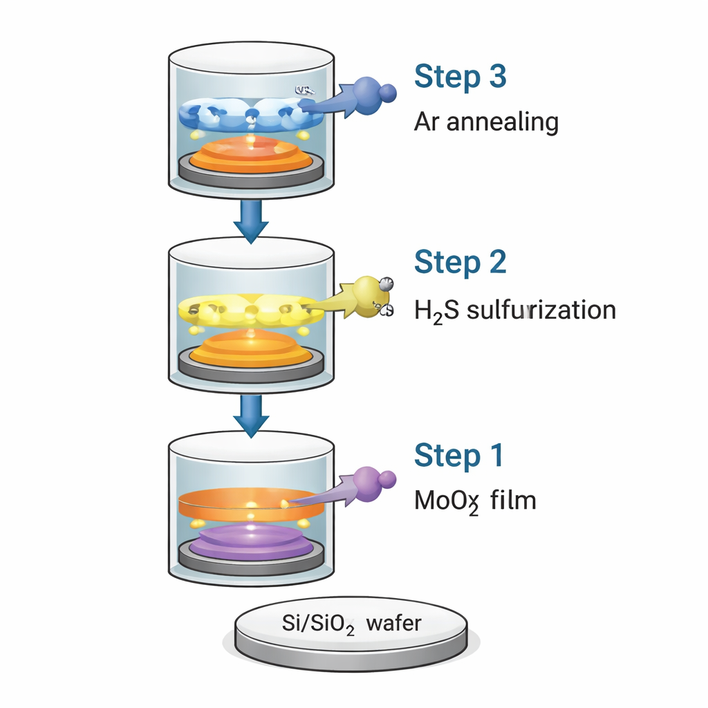
Fine‑Tuning the Starting Material and Conditions
A key insight is that the exact composition of the starting oxide film strongly affects how well it converts into MoS₂. When the oxide contains more oxygen—chemically closer to MoO₃—it transforms more completely and evenly, with less internal stress and fewer defects. Thick oxide layers rich in oxygen sulfurize all the way through, while those with less oxygen leave an unconverted core. The authors explain this in simple physical terms: MoO₃ and MoS₂ have similar volume per atom, so turning one into the other does not force the film to swell much. In contrast, starting from pure metal causes the film to expand strongly when sulfur is added, creating wrinkles and even peeling. Careful control of the gas conditions is just as important. High‑pressure H₂S greatly speeds up sulfur uptake, but if the temperature is too high the hydrogen can actually remove sulfur and damage the film.
From Disorder to Order at the Wafer Scale
To judge how good their MoS₂ films are, the team used optical tools that are standard in semiconductor labs. Raman spectroscopy tracks tiny vibrations of the crystal lattice, while photoluminescence (PL) spectroscopy measures how sharply the film glows when excited by light. They found that a lower signal from disorder‑related Raman features went hand‑in‑hand with a narrower PL peak—signs of fewer defects and more uniform structure. Using this information, they pinned down an optimal window: sulfurization at moderate temperatures under high‑pressure H₂S, followed by a hot argon anneal. Under these conditions, monolayer films showed PL linewidths close to those of single crystals, and thick films rearranged into nicely layered stacks. Importantly, they demonstrated continuous monolayer and bilayer MoS₂ across a full 4‑inch wafer, with only small variations in optical signatures, confirming excellent uniformity. 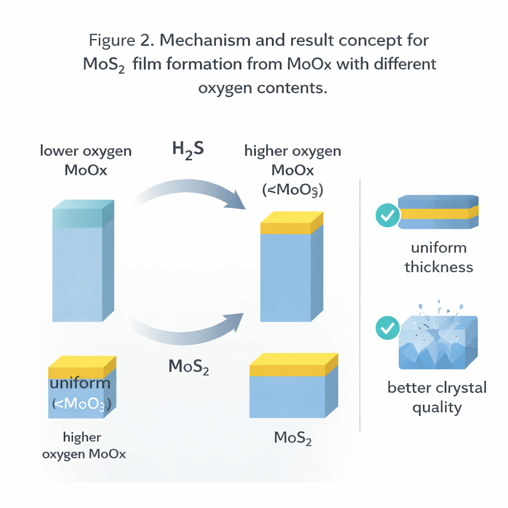
What This Means for Future Devices
For a non‑specialist, the punchline is straightforward: this work turns MoS₂ from a laboratory curiosity into something that can realistically be built into chips and displays. The three‑step method relies on equipment and gases already familiar to the semiconductor industry and offers precise control over film thickness and quality across entire wafers. That means circuit designers can begin to imagine ultrathin, flexible, and energy‑efficient devices that integrate smoothly with today’s silicon technology. If further refined, this approach could underpin a new generation of electronics and optoelectronics based on atom‑thin materials.
Citation: Okada, N., Tanabe, S., Miura, H. et al. Wafer-scale formation of MoS2 with controlled thickness and high uniformity via conversion of MoOx using H2S sulfurization and subsequent crystallization. Sci Rep 16, 7336 (2026). https://doi.org/10.1038/s41598-026-38161-y
Keywords: molybdenum disulfide, 2D semiconductors, wafer-scale growth, thin-film electronics, sulfurization process