Clear Sky Science · en
Facile fabrication of porous BixSy/Si photodetectors by one step laser ablation in liquid
Turning Light into Signals with Tiny Porous Films
From phone cameras to fiber‑optic networks, modern life depends on devices that can sense faint flashes of light and turn them into electrical signals. This paper explores a simple way to make such light sensors—called photodetectors—using a relatively safe, earth‑abundant material, and shows how tuning a laser during fabrication can dramatically boost their performance.
A Gentle Mineral with Powerful Talents
The work centers on bismuth sulfide, a compound that occurs in nature and belongs to a family of materials known for absorbing light efficiently while remaining largely non‑toxic. Bismuth sulfide is especially good at soaking up visible and near‑infrared light—the same ranges used in many imaging and communication technologies. Its internal energy scale, or bandgap, lies in a sweet spot that makes it promising for solar cells and photodetectors. Earlier studies showed that by shrinking this material down to the nanoscale or changing its composition slightly, researchers can tweak how it absorbs and emits light. The challenge has been to make clean, well‑controlled structures without resorting to complex, expensive processing.
Making Nanosponges with a Laser in a Beaker
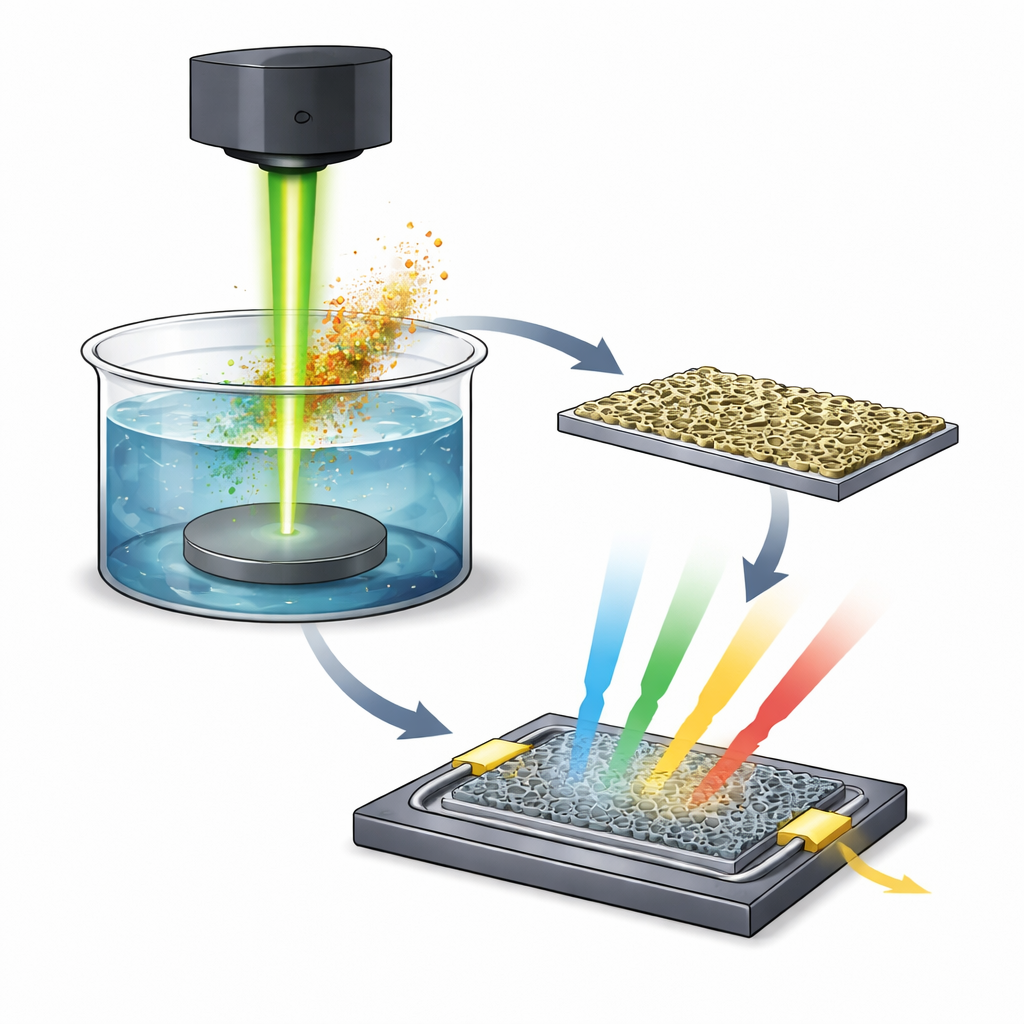
Instead of traditional high‑temperature ovens or chemical baths, the team used a technique called pulsed laser ablation in liquid. They placed a solid bismuth pellet at the bottom of a shallow thiourea solution—a liquid that supplies sulfur atoms—and fired short, intense pulses of green laser light at it. Each pulse knocks atoms off the surface into the liquid, where they meet sulfur and quickly form tiny bismuth sulfide particles. By keeping the number of pulses the same but changing the laser’s energy, the researchers could tune how much material was removed and how the particles grew. The resulting particles were then spun onto silicon wafers as thin coatings, forming a porous, sponge‑like layer on top of the silicon.
From Sponge‑Like Films to Light‑Sensing Chips
Microscope images revealed that these coatings are not smooth skins but intricate three‑dimensional networks of pores and thin walls, with pore sizes on the scale of tens of nanometers. At one particular laser energy, the film resembles a highly uniform grid of interconnected voids covering nearly 80% of the surface. This structure creates a very large internal area where light can be trapped and absorbed, and where electrical charges can be generated. Measurements confirmed that the material formed is crystalline bismuth sulfide, with its internal order improving as the laser energy increases. Optical tests showed that the films’ light‑absorption edge shifts slightly with laser energy, indicating that the size and arrangement of the nanoparticles, as well as small deviations from perfect composition, subtly change how the material interacts with light.
Building and Testing the Light Detectors
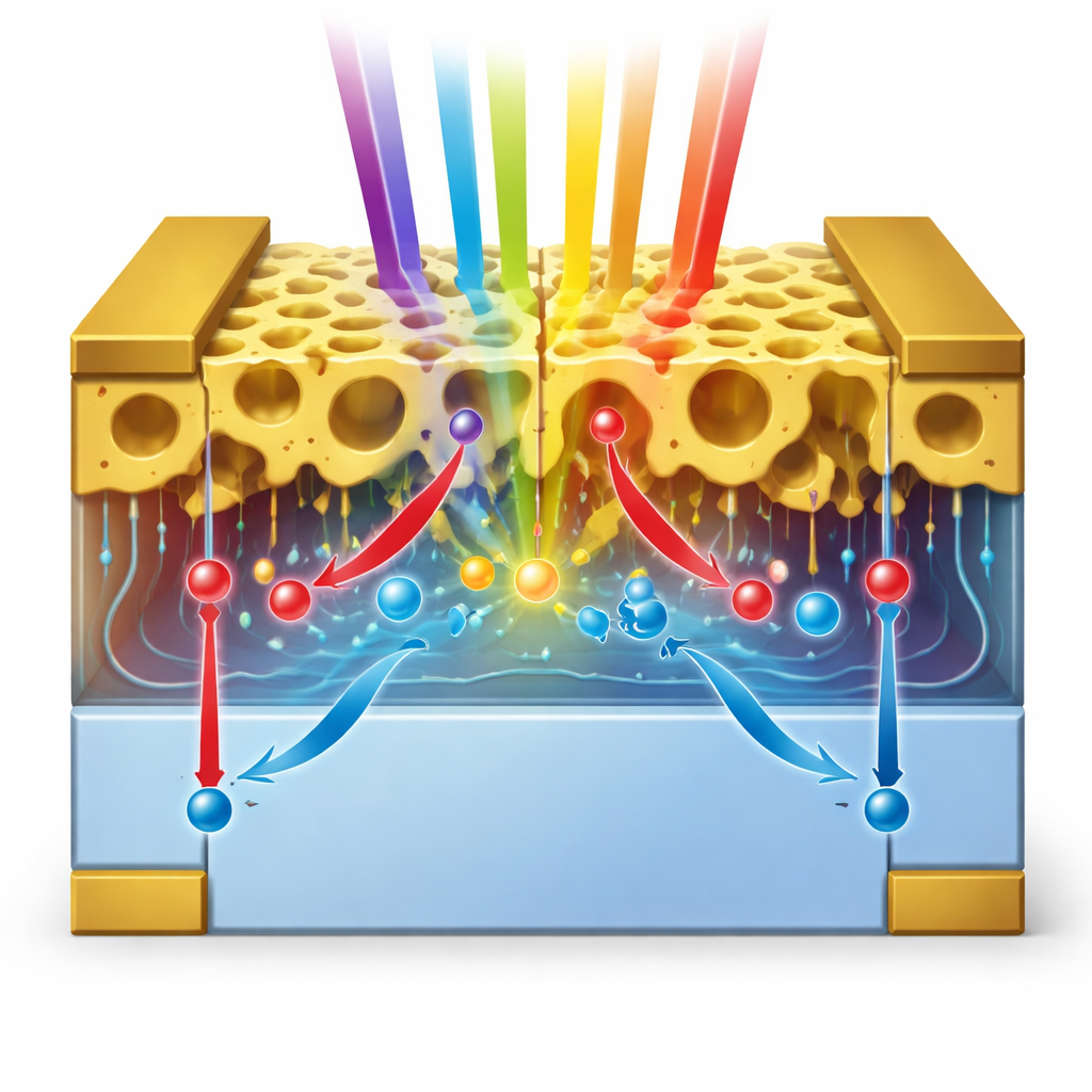
To turn these films into working photodetectors, the researchers sandwiched the porous bismuth sulfide layer between a metal contact on top and a silicon wafer underneath, with another metal contact on the back of the silicon. When light shines on the porous layer, it generates pairs of charges that are separated at the boundary between bismuth sulfide and silicon and swept toward the contacts. By measuring the electrical current that flows under different colors and intensities of light, the team evaluated how responsive each device was. They found that devices made with an intermediate laser energy delivered a strong, nearly linear increase in current with light intensity, high sensitivity to ultraviolet and near‑infrared light, and fast switching between light and dark states. Key performance measures—responsivity, detectivity, and external quantum efficiency—reached values that rival or exceed many previously reported bismuth sulfide devices made by more complicated methods.
Why This Matters for Future Sensors
In plain terms, the study shows that carefully blasting a metal in a simple liquid with a laser can create delicate “nanosponges” that are excellent at catching light and turning it into electrical signals. By tuning the laser’s strength, researchers can control the film’s internal structure and, in turn, how well the resulting detector performs. The best devices in this work are highly sensitive over a broad range of wavelengths, react and recover in fractions of a second, and remain stable over days of operation. Because the method is relatively straightforward, uses a non‑toxic light‑absorbing material, and does not require extra heat treatments or catalysts, it points toward affordable, scalable light sensors for imaging, communications, and low‑power optical detection.
Citation: Ahmed, A.M., Ramizy, A., Ismail, R.A. et al. Facile fabrication of porous BixSy/Si photodetectors by one step laser ablation in liquid. Sci Rep 16, 8047 (2026). https://doi.org/10.1038/s41598-026-37668-8
Keywords: bismuth sulfide photodetectors, pulsed laser ablation in liquid, porous nanostructured films, silicon heterojunction devices, broadband light sensing