Clear Sky Science · en
Optimized electrical and physiochemical properties of cadmium telluride thin films via copper chloride treatment for photovoltaic applications
Why this solar story matters
As the world races to cut carbon emissions, solar power must become cheaper, more efficient, and more reliable in harsh climates. This study explores a way to fine‑tune one of the leading thin‑film solar materials, cadmium telluride (CdTe), using a simple copper salt treatment. By carefully adjusting how much copper chloride is used, the researchers show they can boost the electrical performance of CdTe solar layers while keeping them stable and relatively eco‑friendly, pointing toward better, lower‑cost solar modules.
From sandwiched films to working solar cells
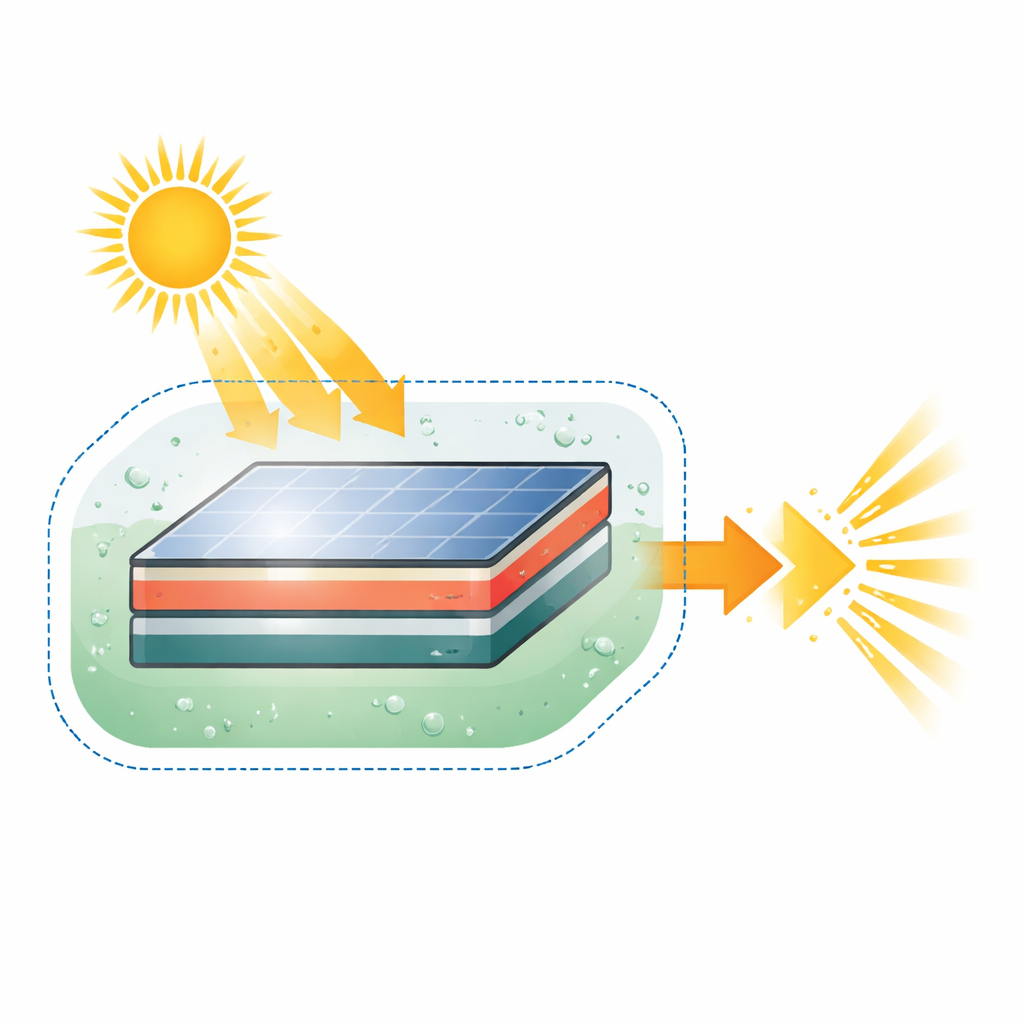
Commercial CdTe solar panels are built as stacks of ultra‑thin layers on glass, with CdTe acting as the light‑absorbing heart of the device. These films are attractive because they perform well in very hot or humid conditions, where standard silicon panels lose power more quickly. However, CdTe devices are often limited by a modest voltage output, tied to how many charge carriers the material can supply and how cleanly they move through the film. The team behind this work set out to improve that balance by using a wet chemical treatment based on copper chloride (CuCl₂), a compound that can introduce helpful electrical dopants while also healing tiny defects in the crystal structure.
Tuning the copper “seasoning”
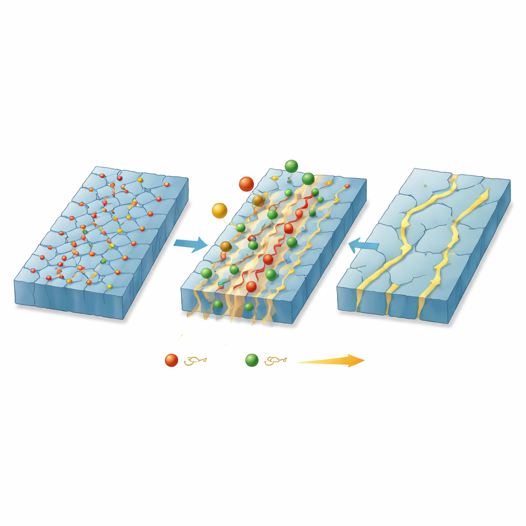
Instead of guessing at a single recipe, the researchers deliberately explored a wide sweep of CuCl₂ concentrations, from very dilute to relatively strong, all applied to CdTe films grown by a high‑temperature method called close‑spaced sublimation. Each sample was dipped in a CuCl₂ solution, briefly rinsed, and then heated in air at 390 °C. This heat step encourages copper and chlorine atoms to move into the CdTe layer and along its grain boundaries—the internal borders between micro‑crystals. The team then used X‑ray diffraction to track how the crystal structure changed, electron microscopy to visualize grain size and texture, and optical and electrical measurements to see how well the films absorbed light and carried charge.
What happens inside the crystal
The crystal studies showed that all treated films kept the same basic CdTe structure, with a strong preference for a particular crystal orientation, and no new copper‑rich phases appeared. At low copper levels, grains tended to be larger and better oriented, with fewer structural defects, but the copper was not active enough electrically to supply many extra charge carriers. As the copper level rose, grain size shrank and internal strain and defect density increased, signaling that too much dopant was beginning to distort the lattice and create new scattering centers. Despite these structural shifts, the optical band gap—essentially the color of light the film can absorb—remained close to its ideal value, meaning the treatment did not undermine the basic light‑harvesting ability of CdTe.
Finding the sweet spot for charge flow
The most striking changes appeared in the electrical tests. Very low copper doses produced films with relatively high resistivity and low carrier concentration, not ideal for a solar absorber. Very high doses, while adding more copper, actually hurt performance by increasing microstrain and defect scattering, limiting how far charges could move before they recombined. In contrast, a mid‑range concentration of 0.005 molar CuCl₂ emerged as the clear optimum. At this level, the films showed the highest carrier concentration, the lowest resistivity, and well‑coalesced grains with fewer boundaries—conditions that favor efficient charge collection and, ultimately, higher solar‑cell efficiency. Follow‑up measurements after a year also highlighted that too much copper tends to diffuse and degrade performance over time, reinforcing the importance of staying near this middle ground.
What it means for future solar panels
To a non‑specialist, the message is that a relatively simple wet treatment—dipping CdTe films in a carefully tuned copper chloride solution and briefly heating them—can act like a smart “tune‑up” for solar materials. At the right dosage, copper helps create more mobile electrical charges and cleans up internal flaws without overloading the crystal with defects. The authors show that 0.005 molar CuCl₂ offers this balance, providing an efficient, solution‑based and less hazardous alternative to older activation methods that rely on more toxic cadmium salts. This kind of optimization at the materials level feeds directly into more powerful, durable, and cost‑effective CdTe solar panels, and the same design principles can guide the development of the next generation of thin‑film photovoltaic technologies.
Citation: Doroody, C., Harif, M.N., Feng, ZJ. et al. Optimized electrical and physiochemical properties of cadmium telluride thin films via copper chloride treatment for photovoltaic applications. Sci Rep 16, 8387 (2026). https://doi.org/10.1038/s41598-026-36991-4
Keywords: cadmium telluride solar cells, thin film photovoltaics, copper chloride treatment, semiconductor doping, renewable energy materials