Clear Sky Science · en
3D LineExplore: a 3D line exploration method for multi-layer PCB geometric routing
Smarter Wiring for the Circuit Boards Inside Everything
Every smartphone, laptop, and car now hides tiny highways of copper that shuttle signals between chips. As electronics cram more parts into less space, drawing these microscopic “roads” on printed circuit boards (PCBs) has become one of the hardest steps in hardware design. This paper presents a new way to automatically plan those routes in three dimensions, promising faster design, fewer errors, and better performance for the devices we use every day.
Why Traditional Routing Hits a Wall
Today’s automatic PCB routers mostly think in terms of a chessboard-like grid: the board is sliced into tiny squares, and algorithms such as A* search for the cheapest path from one pin to another. This works, but it comes with trade-offs. If the grid is coarse, paths are imprecise and may violate design rules. If the grid is very fine, the search explodes in size and becomes painfully slow, especially on multi-layer boards where traces can hop between layers through tiny drilled holes called vias. Gridless methods avoid the artificial grid and work directly with shapes, but so far they have largely been limited to flat, two-dimensional layouts and struggle to handle true 3D, multi-layer routing efficiently.
A 3D “Radar” for Finding Safe Paths
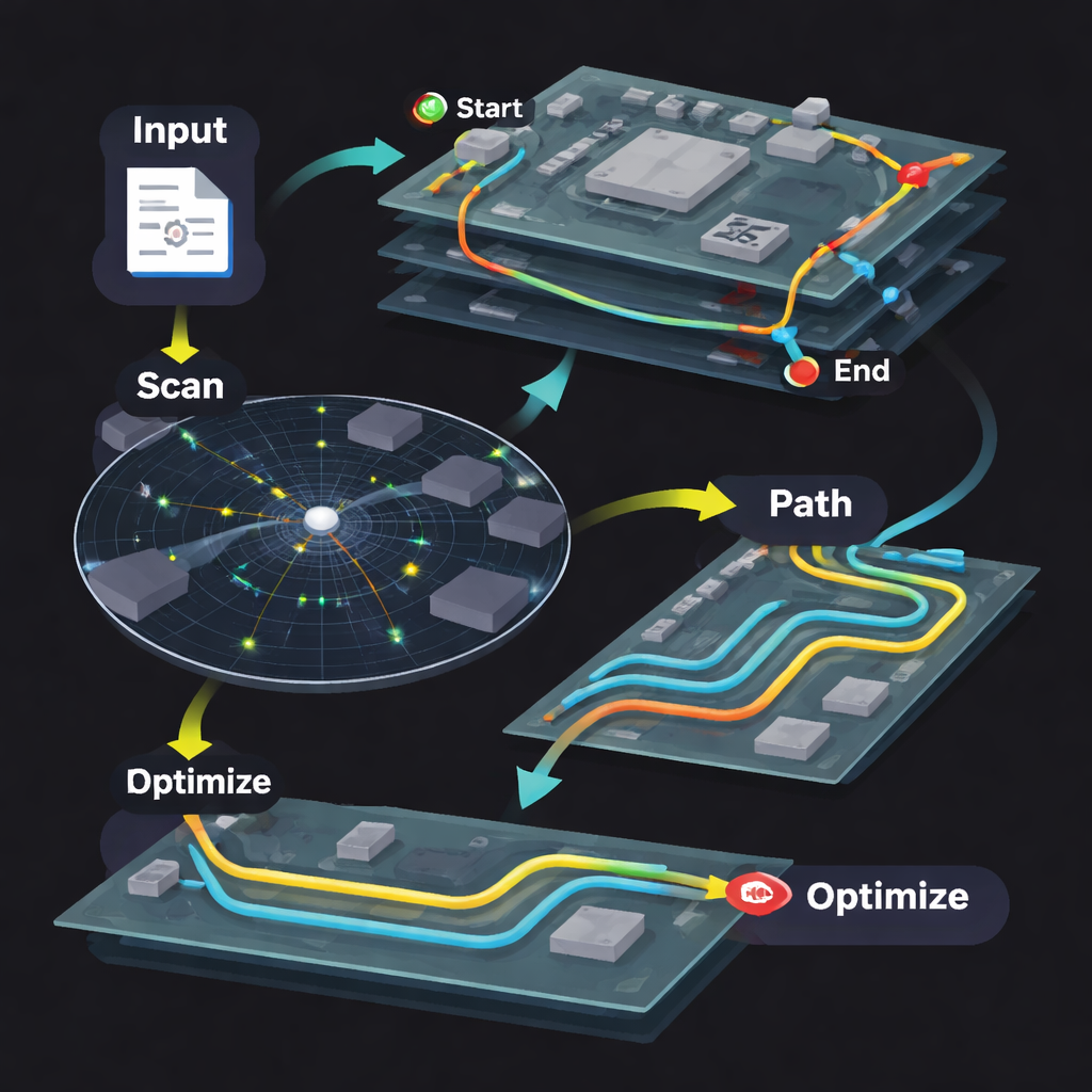
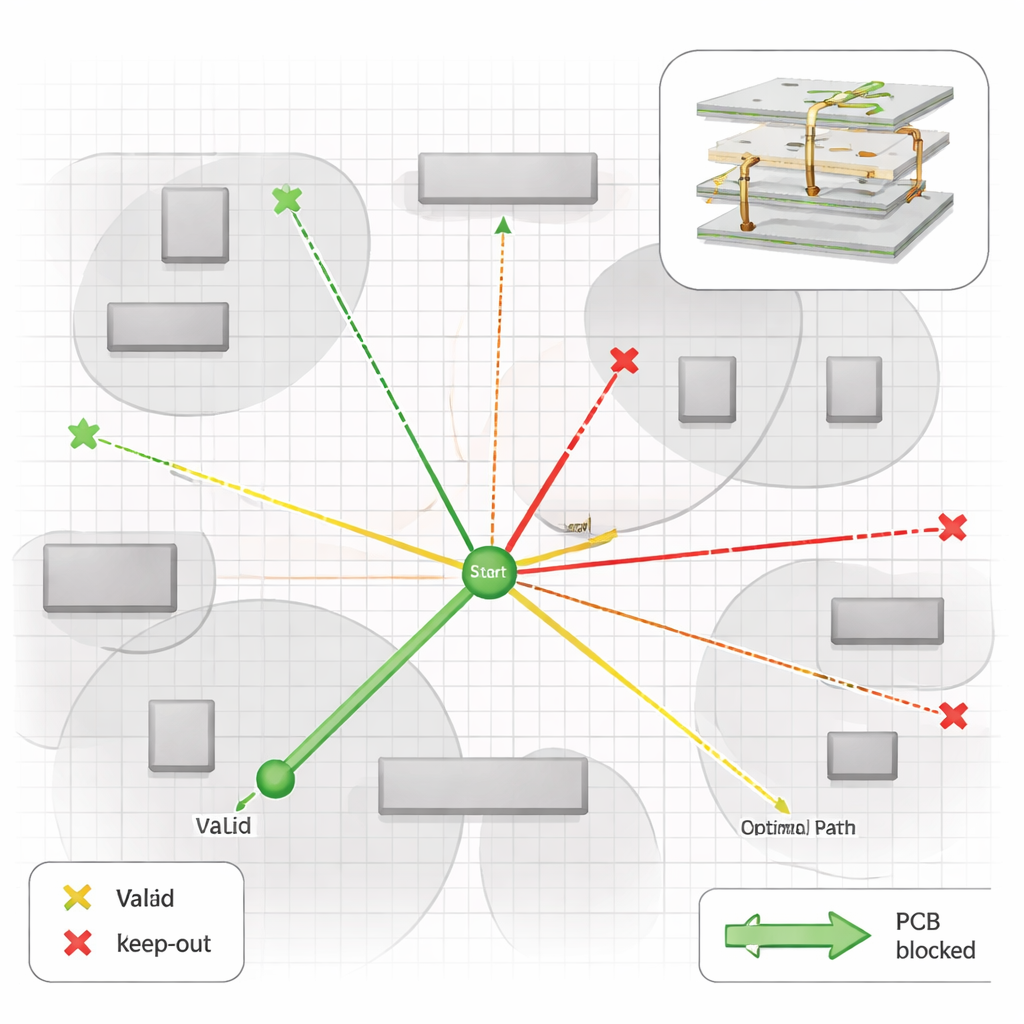
The authors introduce 3D LineExplore, a gridless routing method that works directly in continuous space across multiple layers. At its heart is a “radar”-inspired scanning algorithm. Instead of checking every grid cell, the method looks around the current point in a local neighborhood, identifies nearby obstacles such as components and already-placed wires, and collects key corner points from those shapes. From these, it proposes a compact set of promising “exploration points” where a wire could safely pass. If the immediate neighborhood cannot yield a route, the scan radius expands, but only as needed. This selective probing keeps the search focused, avoids redundant checks, and naturally extends to multiple layers by projecting target points between layers and adding special exploration points that represent potential via locations.
Letting Costs Guide the Best Route
Once the exploration points are known, a second module chooses the actual path. This obstacle-avoidance heuristic path algorithm acts like a guided search: it weighs the distance already traveled, the distance to each next candidate point, the extra cost of drilling a via to another layer, and a straight-line guess of how far remains to the destination. Using these factors in a single cost function and a priority queue, the algorithm always expands the most promising next step. Behind the scenes, this builds a sparse graph of possible moves without ever laying down a full grid. When the target pin is reached, the path is reconstructed by following stored predecessor links back to the start, yielding a complete 3D route that weaves around obstacles and switches layers only when it is worth the added cost.
Cleaning Up Complex Nets and Sharpening the Lines
Real PCBs rarely connect just one pair of pins at a time. Many nets tie three or more pins together, which can easily lead to dead-ends or tangled routes. 3D LineExplore tackles these cases by decomposing a multi-pin net into a sequence of nearest-neighbor pin pairs, routing them one by one, and then repairing any failures. If a connection cannot be completed as planned, the algorithm searches for an alternative attachment to a nearby already-connected pin, restoring the net with minimal extra wire. After all connectivity is secured, a post-processing stage improves the physical shape of the wires. Many high-speed designs prefer bends of about 135 degrees instead of sharp right angles, to ease manufacturing and reduce electrical reflections. The authors introduce a geometric “parallelogram” adjustment that reshapes polyline segments into smoother, 135-degree-constrained paths while preserving all connections and avoiding new collisions.
Putting the New Method to the Test
The team evaluated 3D LineExplore on eleven public benchmark boards ranging from simple to complex, and compared it with both commercial and academic tools, including FreeRouting, ELECTRA, DeepPCB, and an optimized 3D A* algorithm. Across these cases, the new method successfully connected about 98% of required pin pairs, matching or surpassing established routers. More strikingly, its total wire length was, on average, shorter—about 15% less than one leading commercial tool—helping to reduce signal delay and power loss. Although it sometimes used more vias to work around congestion, this trade-off improved space usage and reduced crowding on individual layers. In terms of speed, the one-pass design, combined with adaptive local scanning, allowed most designs to be completed in seconds, and in some settings the adaptive search cut routing time by over 90% compared with a brute-force full-board search, while only slightly increasing wire length.
What This Means for Future Electronics
In simple terms, 3D LineExplore offers PCB designers a way to route dense, multi-layer boards more like a skilled human would: by looking around locally, picking only the most useful candidate routes, and balancing short paths against the cost of changing layers. It avoids the heavy overhead of fine grids while still respecting strict design rules and producing smooth, manufacturable traces. As electronics continue to grow in complexity and shrink in size, approaches like this—especially when combined with future machine-learning guidance—could make automatic routing both faster and more reliable, helping new generations of devices reach the market sooner and work more efficiently.
Citation: Sun, N., Zhang, J., Xu, N. et al. 3D LineExplore: a 3D line exploration method for multi-layer PCB geometric routing. Sci Rep 16, 6588 (2026). https://doi.org/10.1038/s41598-026-36925-0
Keywords: PCB routing, multi-layer boards, gridless algorithm, electronic design automation, 3D path planning