Clear Sky Science · en
Mie-mediated edge-enhanced Raman scattering of vertically-stacking ge quantum-dots/Si-SiN array for enhancing photoluminescence and photodetection
Light on a Chip Gets a Power Boost
As our devices move more data using light instead of wires, we need tiny components on silicon chips that can sense and generate light efficiently, without wasting energy. This study shows how carefully arranged nanoscale crystals of germanium inside silicon can dramatically strengthen light signals, opening paths to faster, low-power communications and ultrasensitive on-chip sensors.
Building Tiny Light Catchers
The researchers created a new three-dimensional structure on standard silicon wafers: vertical stacks of spherical germanium "quantum dots" nestled inside wavy, comb-like silicon ridges coated with silicon nitride. Instead of relying on expensive, ultra-fine patterning, they used a clever combination of etching and thermal processing so that the quantum dots form by themselves and line up with remarkable precision. Each dot is about 40 nanometers across—more than a thousand times thinner than a human hair—and they sit at regularly spaced notches along the ridge sidewalls, both sideways and vertically, forming ordered columns of light-active nanocrystals.
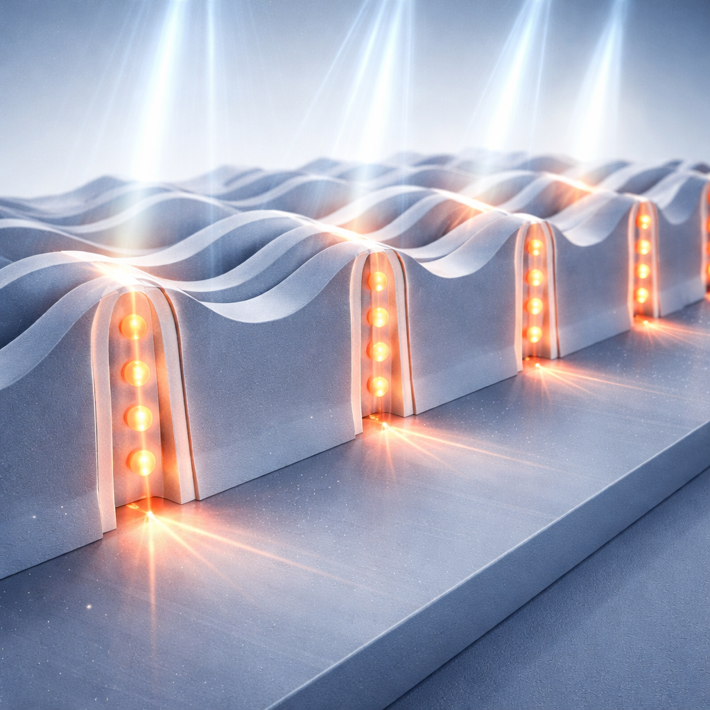
Concentrating Light at Sharp Edges
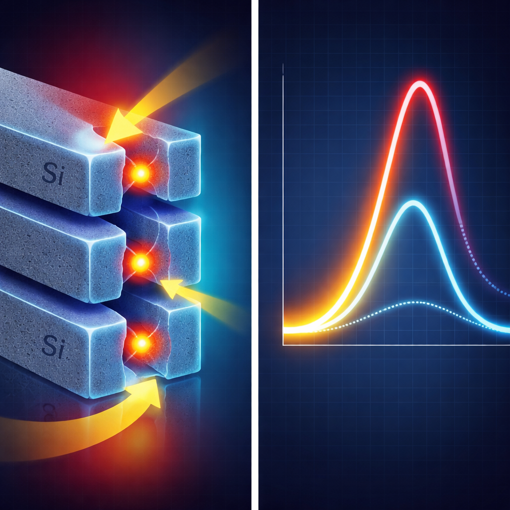
When laser light hits these ridges, the geometry does something special. The wavy edges and stacked quantum dots work together to trap and concentrate the electromagnetic field near the ridge sides. This is detected through Raman scattering, a technique that measures tiny shifts in the color of scattered light and is extremely sensitive to local fields and atomic vibrations. Compared with flat silicon, the corrugated ridges already triple the Raman signal at their edges. Adding the ordered germanium dots boosts the signal up to about fifteen times, especially when the light is polarized along the ridges. This effect, known as edge-enhanced Raman scattering, combines with a resonance effect (Mie resonance) inside the high-index germanium spheres to amplify how strongly the material interacts with light.
Turning Nanostructures into Bright Emitters
These concentrated fields do more than enhance Raman signals—they also strengthen light emission. Using cathodoluminescence and photoluminescence, the team found that the stacked quantum dots emit strongly across the visible and near-infrared spectrum, with sharp peaks around 660 nanometers (red light) and between about 1150 and 1350 nanometers (near-infrared). The emission at shorter wavelength is linked to defects and interfaces that are "lit up" by the nearby quantum dots, while the longer-wavelength band comes from electrons and holes recombining inside the dots themselves. Smaller dots emit more efficiently per unit volume, a hallmark of quantum confinement, where squeezing electrons into a tiny region makes their optical transitions more likely.
Self-Powered Light Detectors Only Atoms Thick
To show that these structures are useful in real devices, the authors built photodiodes—components that convert light into electrical current—using the stacked germanium dots as the active layer. The light-absorbing region is only about 40 nanometers thick, essentially set by the dot size rather than by the limits of the lithography tools. Despite this ultrathin active layer, the detectors achieve low dark current, strong response to light around 850 nanometers, and bandwidths exceeding 20 gigahertz, all at zero applied voltage. The built-in electric field in the device is enough to separate charges, so the detector can operate in a truly self-powered mode, attractive for energy-efficient data links and sensing.
What This Means for Future Chips
In simple terms, this work shows how carefully sculpted silicon structures, seeded with ordered columns of germanium nanocrystals, can bend and concentrate light at scales far smaller than its wavelength. That concentration makes weak signals easier to detect and boosts light emission, enabling compact photodetectors and potential on-chip light sources that run with little or no external power. Because the approach is compatible with silicon manufacturing and stable at high temperatures, it offers a practical route toward densely integrated optical components that could make future computers faster, cooler, and more capable of handling the exploding flow of information.
Citation: Yang, SH., Alonso, M.I., Lin, HC. et al. Mie-mediated edge-enhanced Raman scattering of vertically-stacking ge quantum-dots/Si-SiN array for enhancing photoluminescence and photodetection. Sci Rep 16, 6061 (2026). https://doi.org/10.1038/s41598-026-36743-4
Keywords: silicon photonics, quantum dots, nanophotonics, Raman scattering, photodetectors