Clear Sky Science · en
Tunable multi-band terahertz sensor based on graphene plasmonic metasurfaces
Why this tiny sensor matters
Imagine a medical test or gas detector so sensitive that it can spot minute changes in a sample without needing dyes, labels, or slow chemistry. This paper presents a new kind of ultra-small sensor that works with terahertz (THz) radiation—waves between microwaves and infrared light—and uses a single sheet of carbon, known as graphene, sculpted into a delicate pattern. The result is a tunable, low-cost device that can respond to several signals at once, opening paths toward faster, safer checks for things like blood glucose, exhaled gases, or traces of chemicals.
A new way to read “optical fingerprints”
Many substances—biological tissues, gases, even food products—have unique “fingerprints” in the terahertz range, where their molecules twist, vibrate, or rotate in characteristic ways. Because THz radiation is non-ionizing, unlike X-rays, it can probe delicate samples without damage. The challenge is building sensors that are both extremely sensitive and sharply selective so that tiny changes in a sample’s properties produce clear, measurable signals. Conventional metal-based designs often work in just one narrow band and can be expensive or hard to tune. The authors tackle this by combining THz waves with graphene, whose electrons can be steered electrically, allowing its response to be adjusted after fabrication.
Stacking simple materials into a smart surface
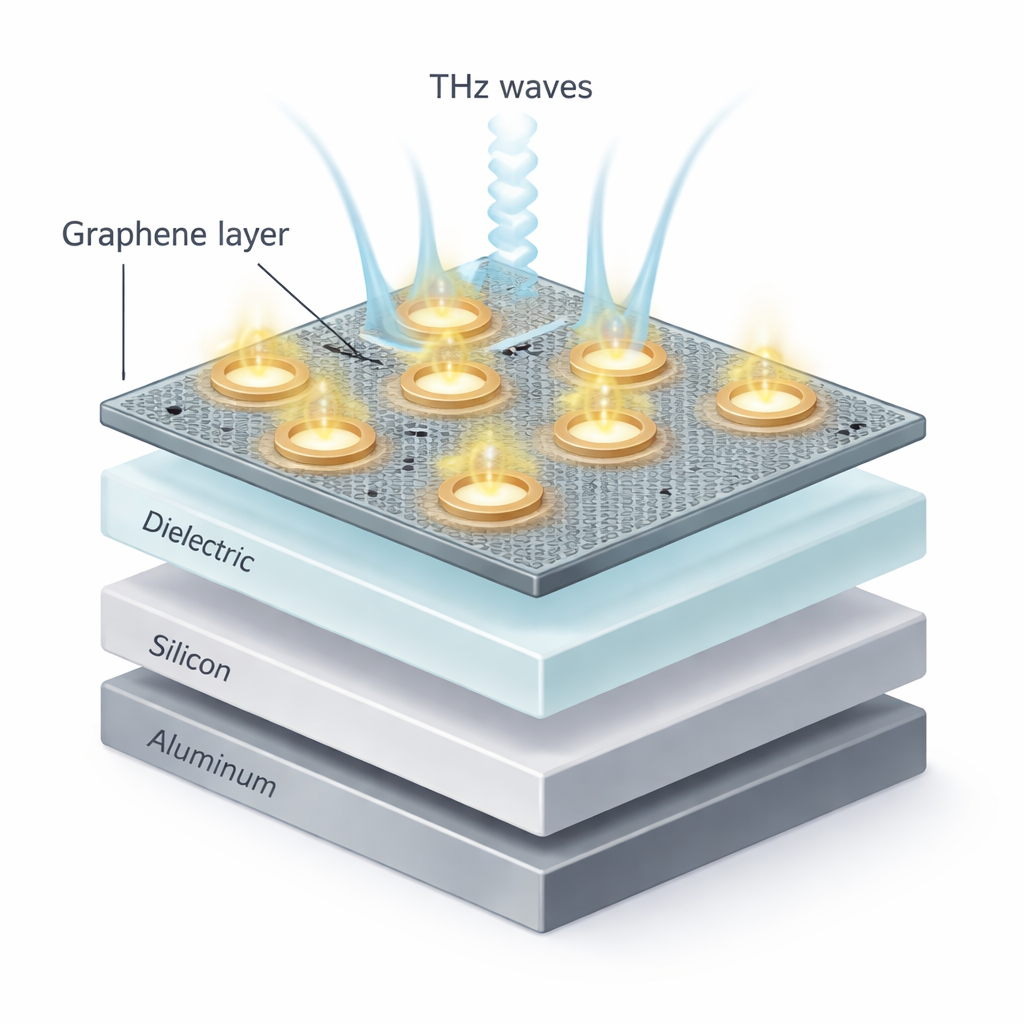
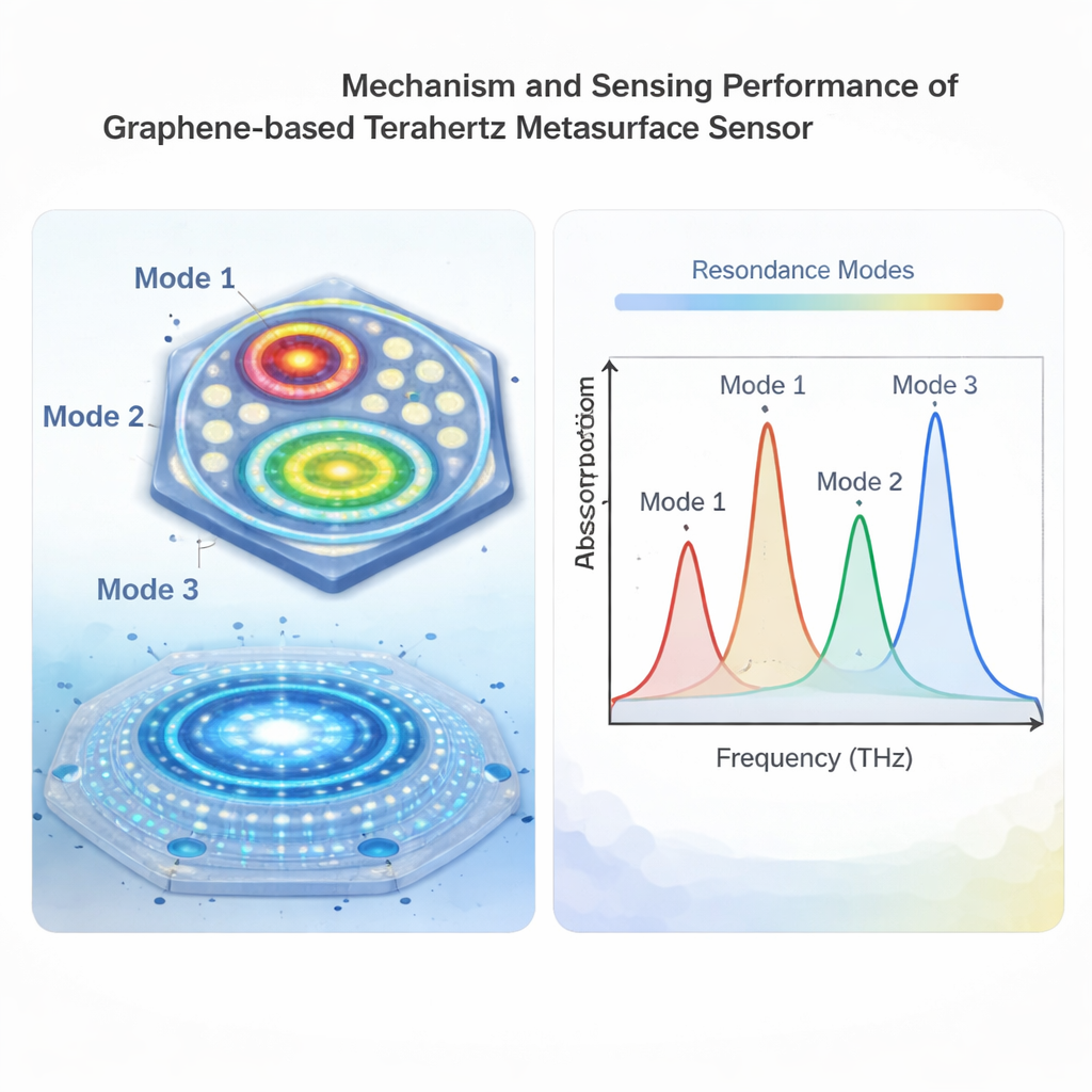
The heart of the device is a carefully engineered stack of everyday materials: a solid aluminum layer at the bottom, a silicon layer, a dielectric (insulating) film, and, on top, a patterned sheet of graphene. This arrangement—metal, dielectric, dielectric, metal—acts like a “metasurface,” an artificial structure that bends and traps light in ways ordinary materials cannot. The graphene is carved into a fractal-like pattern: a central hexagon surrounded by concentric rings and tiny circular patches. When THz waves strike this surface, electrons in the graphene collectively oscillate, forming intense “hot spots” of electromagnetic energy right at the sensor interface. These hot spots are exquisitely sensitive to whatever material—air, liquid, or tissue—touches the surface.
Three colors of sensitivity in one device
A key achievement of this work is that the sensor does not just operate at a single frequency. Instead, its geometry supports three distinct resonant modes, roughly at 7.7, 25.4, and 30.2 terahertz. Each mode acts as an independent sensing channel. When the surrounding material changes—say, its composition or concentration slightly alters its refractive index—these resonant frequencies shift in a nearly linear fashion. The lowest-frequency mode is especially sensitive, with a spectral shift equivalent to 10 micrometers per refractive index unit, while the higher modes offer additional, complementary sensitivities. Because the resonances are narrow and well separated, the device can detect subtle changes with high precision and potentially distinguish between different types of analytes by how they affect each band.
Tuning performance with smart design choices
The authors used detailed numerical simulations to refine every layer and shape in the structure. They showed that using graphene instead of traditional metals reduces energy losses and allows the response to be tuned by adjusting its electronic properties. Adding a silicon layer between the dielectric and aluminum strengthens field confinement and boosts absorption at the key frequencies. They also compared several metals for the bottom layer and found that aluminum offers strong resonances while keeping costs low. By varying parameters like the thickness of the metal and silicon layers and the effective “doping” level of the graphene, they maximized sensitivity and sharpened the resonance peaks, achieving high quality factors and figures of merit that compare favorably with or surpass earlier single- or dual-band designs.
From lab concept to practical tests
Beyond simulations, the study outlines realistic fabrication routes using standard thin-film and lithography techniques already common in the semiconductor industry. Methods such as electron-beam evaporation for aluminum, chemical vapor deposition for graphene, and controlled processes for depositing silicon and dielectric films are discussed, along with known challenges like defects during graphene transfer or alignment limits in patterning. The authors note strategies—such as improved transfer methods and protective coatings—to preserve the sensor’s sharp spectral response in real environments, where contamination or roughness could blur its delicate resonances.
What this means for future sensing
In accessible terms, the work shows how arranging familiar materials in a clever nanoscale pattern can turn a flat surface into a multi-channel “listening post” for terahertz waves. Because the sensor is triple-band, tunable, and made from low-cost components, it offers a promising platform for compact devices that can, for example, monitor blood chemistry, detect trace gases in breath or air, or check moisture and quality in food and industrial products—all without harsh radiation or complex chemistry. While further experimental work is needed, the design points toward a new class of practical, label-free sensors powered by graphene and terahertz metasurfaces.
Citation: Khafagy, M., Ghanim, A.M. & Swillam, M.A. Tunable multi-band terahertz sensor based on graphene plasmonic metasurfaces. Sci Rep 16, 5938 (2026). https://doi.org/10.1038/s41598-026-36617-9
Keywords: terahertz sensing, graphene metasurface, refractive index sensor, plasmonic biosensor, multiband absorber