Clear Sky Science · en
Enhancing uniformity in HARC etching via edge bias voltage and structural impedance variations in a rectangular voltage waveform
Why chip makers care about straight holes
Modern memory chips squeeze more information into smaller spaces by drilling billions of ultra-deep, pencil-thin holes into silicon. These "high-aspect-ratio" holes must be almost perfectly vertical; even slight leaning or shape distortion can ruin a device and slash production yield. This paper shows a new way to keep those holes straight and uniform across an entire silicon wafer by fine-tuning how electric fields act at the wafer’s edge during plasma etching.
The problem with the wafer’s fragile border
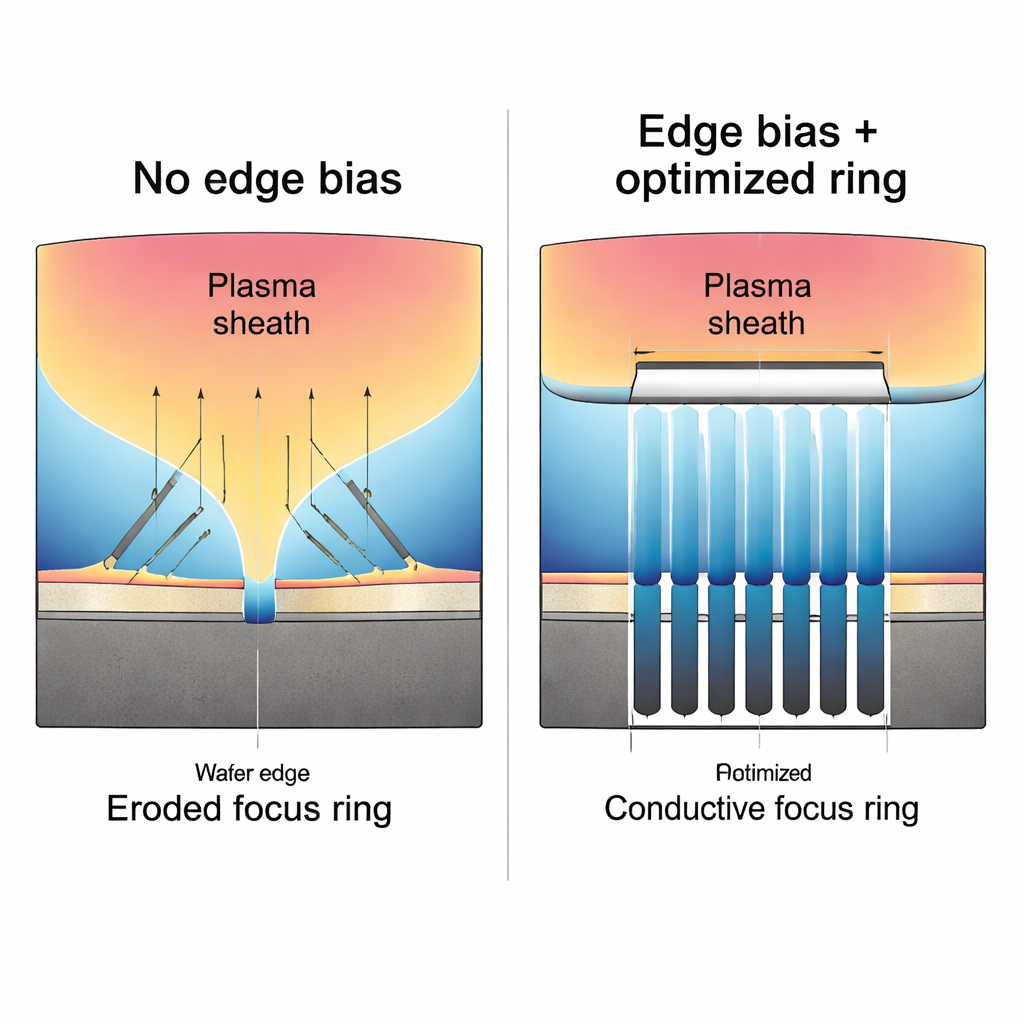
To carve patterns into a wafer, manufacturers use a plasma — a glowing gas full of energetic ions that blast away material. Around the wafer sits a sacrificial "focus ring" that helps keep the plasma even from center to edge. Over time, this ring is eaten away by the same harsh environment that etches the chip. As it erodes, the electric sheath that guides ions toward the wafer becomes warped near the edge. Instead of hitting straight down, ions arrive at an angle, making holes tilt toward the center and stretch into ellipses. This not only distorts the tiny capacitor structures but also reduces usable area and lowers yield.
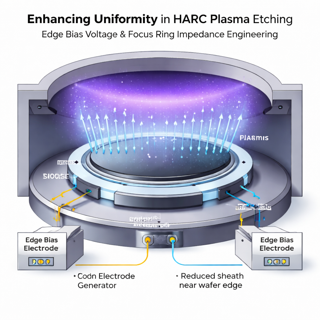
Adding a controllable "steering wheel" at the edge
The researchers tackled this by adding an independently controlled edge electrode beneath the focus ring, powered with a rectangular-shaped bias voltage separate from the main wafer bias. Rather than the usual smooth sine wave, this square-like waveform switches sharply between on and off, keeping the voltage difference between the plasma and the surface more constant in time. That steadier push lets ions arrive with a narrower range of energies and angles. By carefully raising the edge bias, the team could strengthen and reshape the electric sheath at the wafer rim, pulling ion paths back toward vertical and recovering circular, well-defined trench profiles even where the focus ring had worn down.
When more power makes things worse
However, turning up the edge voltage too far created a new problem. Above about 280–300 volts, electrical interaction between the edge and center electrodes caused unwanted current to leak through the plasma. Monitors showed growing mismatches between the voltage the equipment tried to apply and the actual voltage seen by the wafer, along with rising currents in the wafer region. This disturbed the carefully tuned sheath, making the plasma unstable and reintroducing non-uniform etching: middle regions etched faster, the edge slowed down, and hole shapes again became distorted despite the higher edge bias.
Redesigning the hardware to tame the fields
To restore control at high voltages, the team re-engineered the stack of insulating and conductive parts around the wafer — especially the materials under and around the focus ring. By swapping components and changing their electrical properties, they adjusted the impedance ratio between the focus ring path and the wafer chuck. A higher ratio (about 1.31) limited unwanted coupling between the two bias circuits, allowing the edge bias to do its job without dragging the center along. Experiments showed that with this optimized configuration, trenches stayed nearly circular and vertical even at 300 volts edge bias, and the etch rate stayed much more uniform across the wafer. Computer simulations backed this up, revealing how different focus ring materials (silicon versus quartz) change sheath thickness, plasma density, and the strength of the vertical electric field.
What this means for future memory chips
For non-specialists, the key message is that the authors have found a way to "steer" the invisible electric fields at a wafer’s edge so that plasma ions drill straighter, more consistent holes. By combining a separately controlled, rectangular edge bias with an electrically optimized support structure, they can both correct edge tilt and avoid instabilities that come from pushing voltages too high. This approach should help manufacturers keep etching precise, deep features as memory cells continue to shrink, improving yield and reliability in next-generation semiconductor devices.
Citation: Park, C., Cho, J., Um, J. et al. Enhancing uniformity in HARC etching via edge bias voltage and structural impedance variations in a rectangular voltage waveform. Sci Rep 16, 5851 (2026). https://doi.org/10.1038/s41598-026-36323-6
Keywords: plasma etching, semiconductor manufacturing, high aspect ratio, edge bias voltage, focus ring design