Clear Sky Science · en
FDTD-based design of high quality factor quantum dot photonic crystal nanolaser for next-generation nanotechnologies
Lighting up the tiniest devices
From medical sensors smaller than a grain of sand to future quantum computers, many emerging technologies need light sources that are both incredibly small and remarkably efficient. This paper describes a new kind of "nanolaser" built from carefully patterned semiconductor layers. The device squeezes light into a space smaller than the width of a human hair while wasting very little energy, and it is designed not only to shine but also to plug directly into quantum logic circuits that process information in fundamentally new ways.
Building a laser on a chip
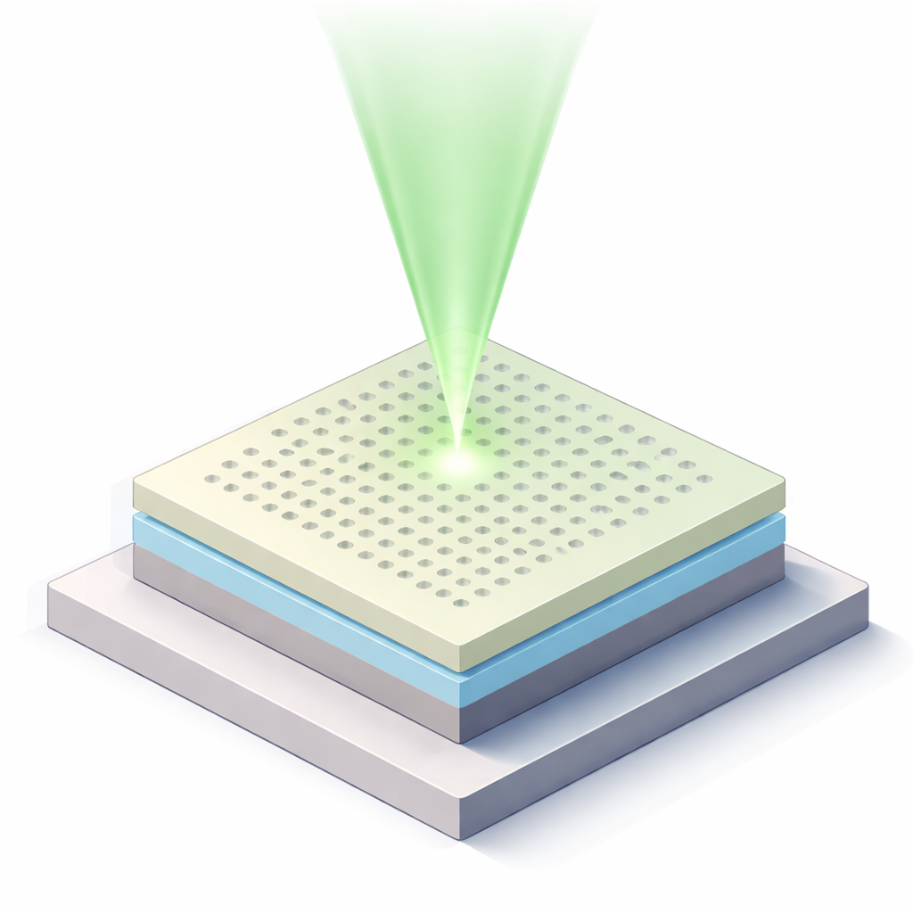
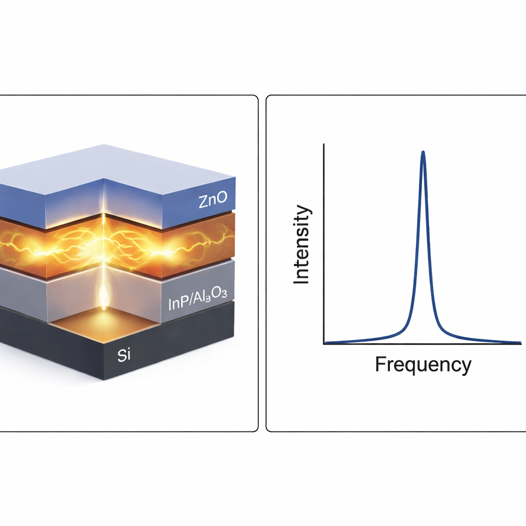
The researchers start with a flat silicon chip and stack ultra-thin layers of indium phosphide (InP), aluminum oxide (Al₂O₃), and zinc oxide (ZnO) on top. They then drill a precise triangular array of tiny air holes through the top region, forming what is known as a photonic crystal. Just as a regular crystal can control how electrons move, this man-made "crystal of holes" controls how light moves. By leaving carefully placed imperfections—called defects—in this pattern, the team creates a tiny optical cage that traps light in an extremely small volume right where quantum dots, the light-producing islands, are located.
Why the material mix matters
Traditional nanolasers based only on common compound semiconductors like InP or GaAs often suffer from leakage of charge carriers, unwanted heat, and blurred emission colors. The new design combines InP quantum dots with a wide-bandgap material, ZnO, separated and shaped with thin Al₂O₃ layers. ZnO is especially attractive because it can handle strong excitation, has stable light-emitting properties, and can be grown as nanorods, nanowires, or films. In this hybrid stack, Al₂O₃ helps confine the optical field in the gain region while reducing surface defects that normally absorb light. Simulations that include realistic optical properties of all layers show that this combination greatly reduces loss, improves light confinement, and boosts the so‑called quality factor—a measure of how long light can bounce around inside the cavity before dying out.
Squeezing more light from fewer photons
Inside such a tiny cavity, the rules of light emission change. The authors make use of the Purcell effect, where placing quantum dots inside a high-quality, small-volume cavity speeds up their spontaneous emission and channels it into a preferred direction and color. By tuning the ratio of the hole size to the lattice spacing and accounting for how the materials’ optical properties vary with temperature, they reach quality factors up to about 1600 for the InP layer and even higher in the full InP/Al₂O₃/ZnO structure. Their calculations show sharp emission peaks at specific infrared and terahertz frequencies, along with reduced threshold current—meaning the laser can turn on with less input power. Compared with earlier nanolaser designs reported in the literature, the proposed device offers both higher quality factors and lower dispersion, indicating more stable and cleaner laser operation.
From bright dots to quantum logic
Beyond acting as a tiny light source, the authors demonstrate how the laser’s output can feed directly into quantum logic gates, the building blocks of quantum computers. They study how light pulses from the nanolaser drive rotations of quantum bits (qubits) and how changing the phase of special gates, such as the Rz and CNOT gates, affects qubit states over time. Using models inspired by Rydberg-atom systems and tests on IBM’s quantum hardware, they explore how errors—especially correlated phase errors that strike two qubits at once—can be detected and corrected using an additional “helper” qubit. Quantum state and process tomography techniques then reconstruct how faithfully the implemented quantum gates behave, with the optimized phase-control scheme reaching gate fidelities as high as about 99.6%.
What this means for future technologies
For non-specialists, the key message is that this work brings together two fast-moving fields: ultra-compact lasers and practical quantum computing. By designing a nanolaser that not only traps light with exceptional efficiency but also couples naturally into quantum logic operations, the authors outline a realistic route toward chip-scale systems where light both carries and processes quantum information. In simple terms, they have engineered a tiny, energy-saving laser that can talk the "language" of qubits, making it a promising building block for next-generation optical sensors, secure communication links, and scalable quantum processors.
Citation: Farmani, A., Omidniaee, A. FDTD-based design of high quality factor quantum dot photonic crystal nanolaser for next-generation nanotechnologies. Sci Rep 16, 6985 (2026). https://doi.org/10.1038/s41598-026-36019-x
Keywords: nanolaser, photonic crystal, quantum dots, quantum logic gates, zinc oxide