Clear Sky Science · en
Engineered fano resonances in a compact Si3N4 photonic crystal nanobeam-microring platform for multi-cladding environments
Sharper Light for Smaller Sensors
From medical diagnostics to environmental monitoring, many modern sensors work by watching how light changes as it passes through tiny structures on a chip. This paper explores a way to make those changes much sharper and easier to read, using a special kind of optical effect called a Fano resonance. The result is a compact, robust sensor platform that can work both in air and in liquid, promising simpler and more sensitive lab-on-a-chip devices for detecting changes in the surrounding medium.
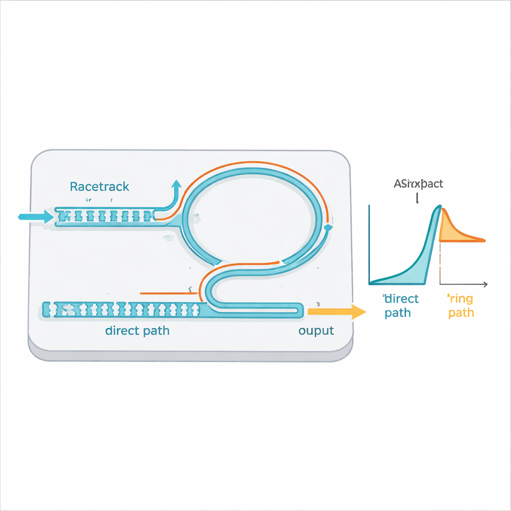
A Tale of Two Light Paths
At the heart of this work is a miniature optical circuit built from silicon nitride, a material compatible with standard chip manufacturing. The device combines two elements: a racetrack-shaped microring resonator and a straight, slotted waveguide called a photonic crystal nanobeam. Light entering the chip can follow two main routes. One part travels directly through the slotted waveguide, forming a smooth background signal. Another part is coupled into the microring, where it circulates many times at particular colors (wavelengths), creating very narrow resonances. When these two pathways meet again at the output, their signals add or cancel in a wavelength-dependent way, producing the characteristic asymmetric Fano lineshape—an abrupt, skewed dip-and-peak pattern in the transmitted light.
Making Fano Behavior Tunable and Robust
The researchers focus on turning this complex interference into a practical design tool rather than an accident of fabrication. They control the device response using only geometry: the length of the slotted nanobeam (how many rectangular slots it has) and the gap between the nanobeam and the microring. These parameters set how strongly the ring interacts with the background pathway and how much light the nanobeam transmits or scatters. Using analytical theory, computer simulations, and experiments, the team shows how these geometric knobs tune key features of the Fano resonance—its asymmetry, depth, and especially the steepness of its slope near the inflection point, where a tiny wavelength shift produces a large change in intensity. They also introduce simple slope-based figures of merit to compare designs without needing to extract every microscopic detail.
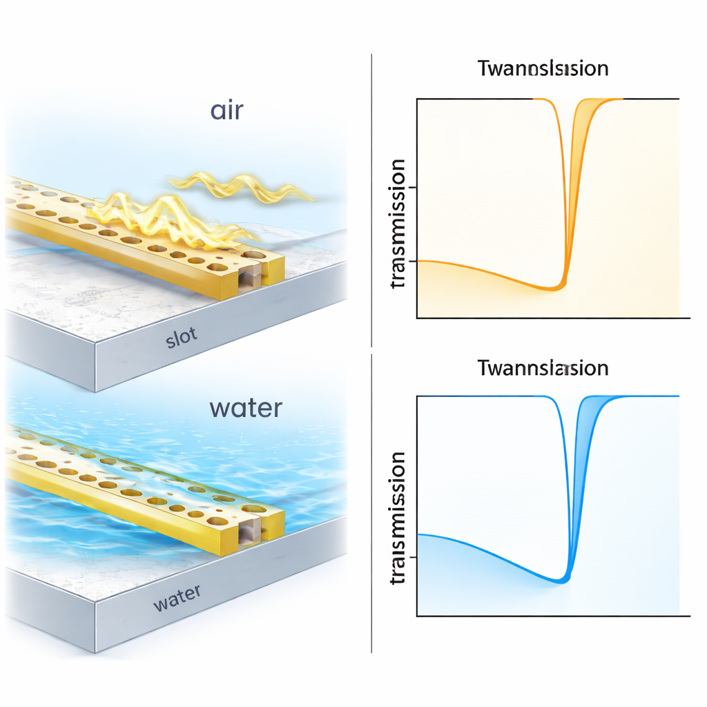
One Chip, Two Environments
A major challenge for practical sensors is that they often must work both in gases and in liquids, which have very different optical properties. In air, the light traveling in the slotted nanobeam leaks more strongly into the surroundings, acting like a “leaky” background channel. When the same chip is covered with water, the refractive index contrast changes and that background mode becomes more tightly guided. Remarkably, the authors show that their design still produces clear, controllable Fano resonances in both cases. Measurements under air and deionized water claddings confirm that the overall behavior—sharp, asymmetric lineshapes with high contrast—matches the theoretical model. The quality factor, asymmetry, and extinction ratio remain in a favorable range, even though the device footprint is just about 40 by 34 micrometers, much smaller than the width of a human hair.
From Lineshapes to Practical Sensing
Beyond demonstrating attractive optical spectra, the study emphasizes what matters for sensing: how quickly the transmission changes with wavelength. The team quantifies this slope and shows that the engineered Fano resonances can reach responsivities above 5 inverse nanometers, corresponding to roughly 40–50 decibels of intensity change per nanometer of wavelength shift. Importantly, they achieve this without pushing for extreme quality factors or ultra-deep notches, which are often difficult to fabricate reliably. Instead, moderate asymmetry and extinction are combined with careful geometric tuning to give a steep yet robust response, suitable for measuring small refractive index changes in real-world lab-on-chip systems.
Why This Matters for Future Lab-on-a-Chip Devices
In simple terms, this work shows how to design tiny on-chip optical structures so that a small environmental change—like a shift in the refractive index when a chemical or biomolecule binds near the surface—creates a large, easy-to-measure intensity signal. By providing clear design rules that connect geometry, surrounding medium, and spectral slope, the authors turn Fano resonances from a curious spectral feature into a practical engineering tool. Because the platform is compact, compatible with standard chip technology, and operates reliably in both air and liquid, it offers a promising foundation for next-generation photonic sensors in medical diagnostics, environmental analysis, and other applications where fast, sensitive, and scalable optical readout is essential.
Citation: Mendoza-Castro, J., Vorobev, A.S., Iadanza, S. et al. Engineered fano resonances in a compact Si3N4 photonic crystal nanobeam-microring platform for multi-cladding environments. Sci Rep 16, 7347 (2026). https://doi.org/10.1038/s41598-026-35490-w
Keywords: Fano resonance, photonic sensors, microring resonator, silicon nitride photonics, lab-on-a-chip