Clear Sky Science · en
Interpreting artificial neural network-based modeling of 4 H-SiC mosfets using explainable AI
Smarter Power Electronics for Everyday Technology
From electric cars to renewable energy plants, modern life increasingly depends on power electronics that can switch electricity efficiently and reliably. A promising class of devices made from silicon carbide (SiC) can handle higher voltages and temperatures than traditional silicon, but they are difficult and expensive to optimize. This study shows how a combination of neural networks and explainable artificial intelligence can speed up the design of these devices while still letting engineers understand what the models are doing under the hood.
Why Tough Power Switches Matter
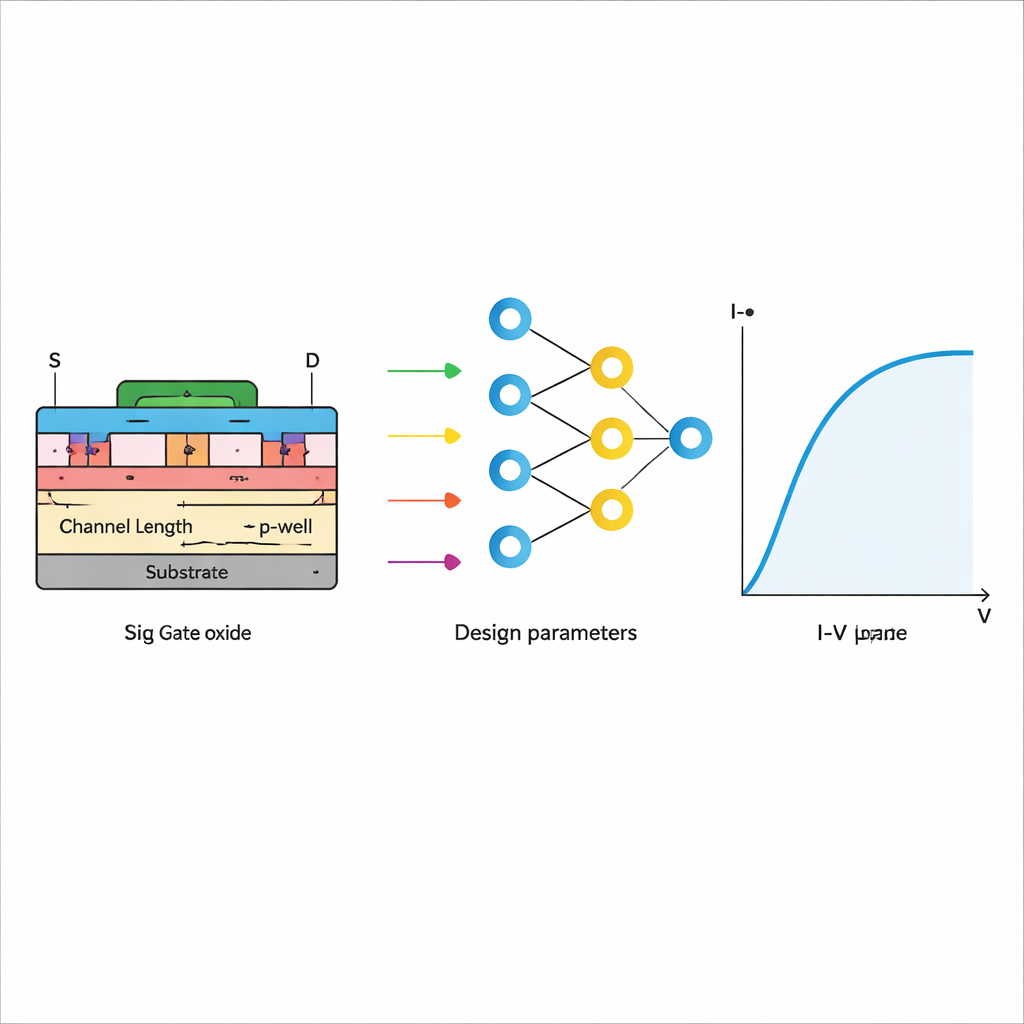
Power switches based on wide bandgap materials like 4H‑SiC metal–oxide–semiconductor field‑effect transistors (MOSFETs) are at the heart of high‑voltage electronics. They promise more efficient chargers for electric vehicles, smaller power converters for solar panels, and robust drives for industrial motors. Yet tuning their internal structure—such as how thick the insulating layer is, how long the channel is, and how strongly different regions are doped with impurities—requires many costly fabrication steps or heavy computer simulations. Traditional device simulators can predict performance in detail, but running thousands of such simulations for design exploration quickly becomes impractical.
Turning Simulations into a Fast Digital Surrogate
The authors tackle this problem by first generating a large library of simulated devices using an industry‑standard tool called TCAD. They systematically vary five key design knobs: the oxide thickness between the gate and channel, the channel length, and the doping levels in the p‑well, drift region, and substrate. For each virtual device they compute how the electric current responds as the gate voltage is swept, producing 3,000 detailed current–voltage curves. This rich dataset becomes the training ground for an artificial neural network, which learns to mimic the simulator’s predictions. Once trained, the network can predict the current for new combinations of design parameters almost instantly, yet with accuracy high enough that the correlation with the original simulations exceeds 0.99 for the on‑state current.
Opening the Black Box with Explainable AI
High accuracy alone is not enough for engineers who must justify design choices in terms of underlying physics. Neural networks are often described as “black boxes” because it is hard to see how each input contributes to the final output. To make their model transparent, the researchers apply a method from explainable AI known as SHAP, which borrows ideas from cooperative game theory. SHAP assigns a numerical “credit” to each design parameter for every prediction the network makes. By examining these scores across all samples, the team can see not only which parameters matter most, but also whether they tend to increase or decrease the current.
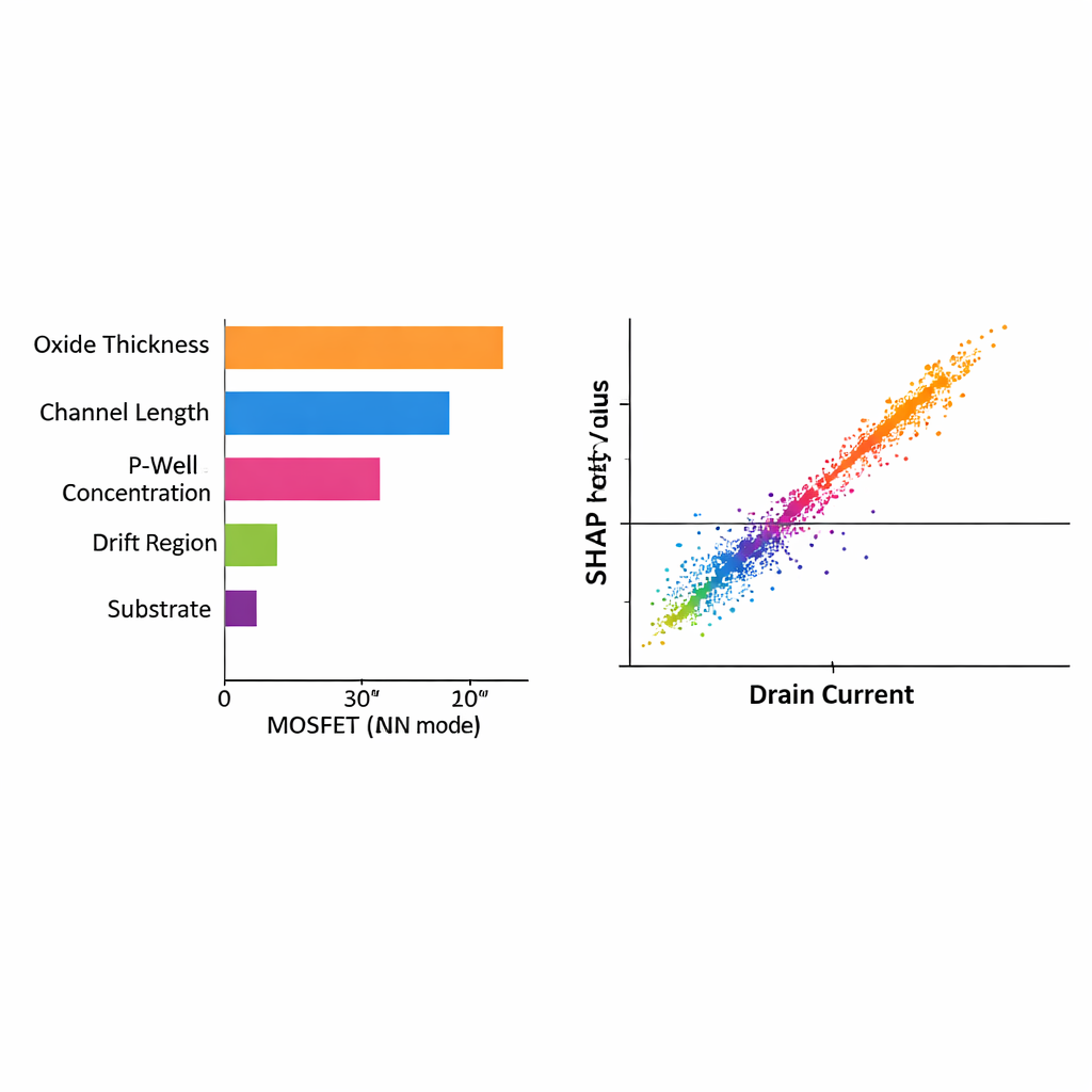
What the Model Learns About Device Physics
The SHAP analysis reveals trends that line up neatly with textbook device physics. Changes in channel length, oxide thickness, and p‑well concentration all have strong and systematic effects on the drain current predicted by the model. Thicker oxide and longer channels, for example, receive SHAP scores that correspond to lower current, matching the expectation that they hinder charge flow. In contrast, variations in the drift region and substrate doping show almost zero SHAP contribution under the tested operating condition, indicating they mainly influence high‑voltage blocking rather than the on‑state current. The authors further distinguish between global interpretability—how each parameter affects the full current–voltage curve across the dataset—and local interpretability, which examines specific combinations of parameters. In both views, SHAP tracks closely with the simulated current, reinforcing confidence that the neural network has captured the correct physical relationships rather than spurious patterns.
A Transparent Roadmap for Future Device Design
Taken together, this work offers a template for designing advanced semiconductor devices in a way that is both fast and trustworthy. The neural network serves as a high‑speed stand‑in for heavy simulations, while the SHAP analysis acts as a lens that reveals which design choices truly drive performance. For non‑specialists, the key message is that AI does not have to replace physical understanding; it can instead highlight and quantify the same trends that engineers expect, and do so across thousands of possible designs. The same framework could be extended to other power devices and emerging materials, helping bring more efficient, reliable electronics into everyday technologies more quickly and at lower development cost.
Citation: Hsiao, YS., Chang, PJ., Chen, BR. et al. Interpreting artificial neural network-based modeling of 4 H-SiC mosfets using explainable AI. Sci Rep 16, 5297 (2026). https://doi.org/10.1038/s41598-026-35179-0
Keywords: silicon carbide MOSFETs, power electronics, neural networks, explainable AI, device modeling