Clear Sky Science · en
Fast photo-carrier multiplication by engineered potential trap in MoS2/Ge double junction phototransistor
Seeing Clearly Through Fog and Darkness
Imagine car cameras, security systems, or medical scanners that can see through fog, haze, or moonless nights as easily as through a sunny afternoon—without relying on bulky, expensive military-grade sensors. This research introduces a new kind of ultra-sensitive, fast-acting light sensor that can detect both visible light and short-wave infrared (SWIR) light, the part of the spectrum that cuts through bad weather and darkness. By cleverly stacking two different semiconductor materials, the authors build a tiny device that multiplies incoming light signals without slowing down, pointing the way toward sharper, cheaper, and more reliable imaging systems.
Why Invisible Light Matters
Short-wave infrared light, with wavelengths roughly between 1 and 3 micrometers, behaves differently from the light our eyes see. It scatters less in fog and haze, and it can make use of faint natural glow in the night sky, enabling clearer vision in darkness. That makes SWIR cameras attractive for self-driving cars, medical imaging, semiconductor inspection, astronomy, and face recognition. Today, many of these tasks rely on detectors made from an alloy called InGaAs, which must be grown on costly wafers and still offers limited sensitivity unless additional electronics provide gain. Cheaper, more versatile materials like graphene, quantum dots, and exotic thin crystals have been explored, but they often lean on random charge traps inside the device to boost the signal—leading to sluggish response times that are unsuitable for fast imaging.
Building a Smarter Light Trap
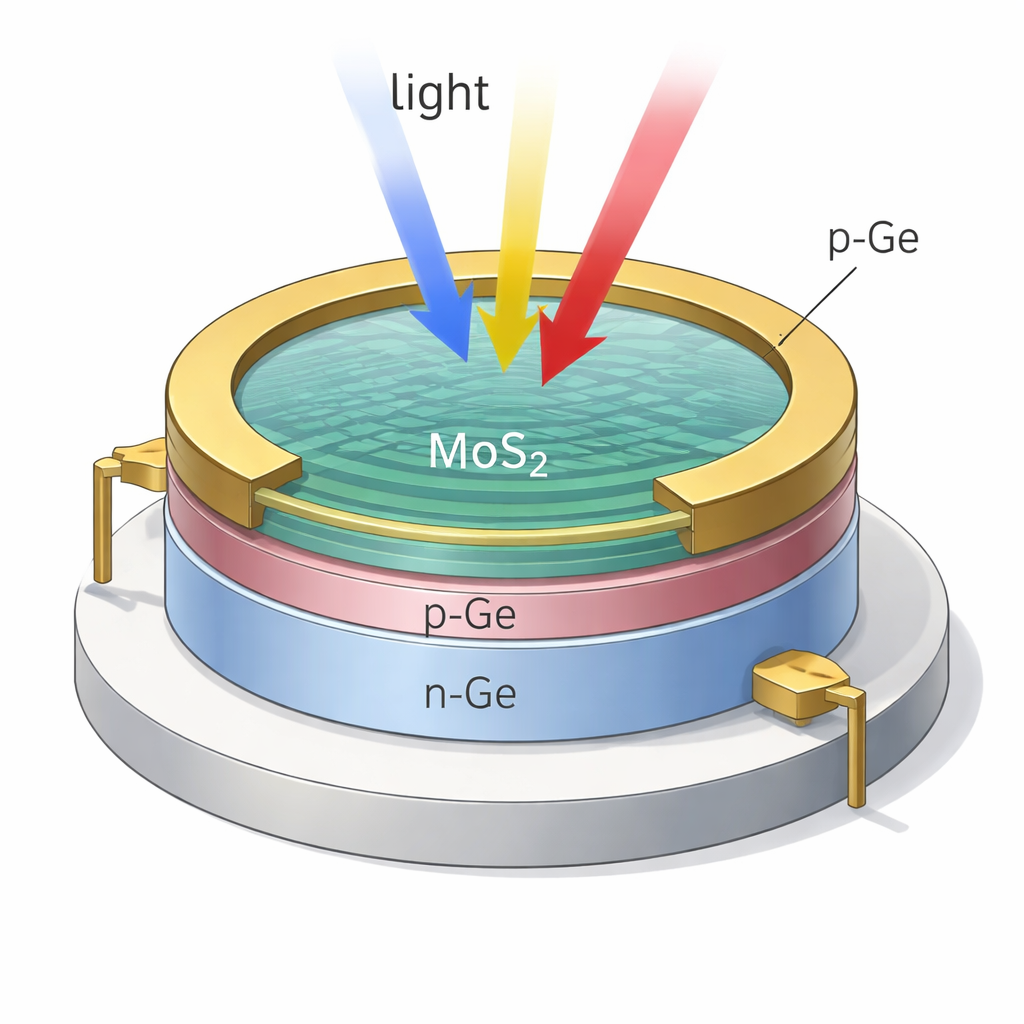
The authors solve this speed–sensitivity trade-off by designing an intentional “potential trap” for electric charges rather than relying on accidental defects. Their device combines a very thin, layered crystal of molybdenum disulfide (MoS2) with germanium (Ge), a well-known semiconductor used in optics and electronics. MoS2 is excellent at absorbing visible light, while Ge strongly absorbs SWIR; together they cover a broad range of wavelengths. The researchers first create a tiny junction inside Ge by forming a thin p-type region on top of n-type Ge. They then place a multilayer MoS2 flake on this p-type layer, forming a second junction. The shared p-type Ge region effectively becomes the “base” sandwiched between MoS2 (the emitter) and n-type Ge (the collector), much like a transistor designed specifically for light.
How One Particle Triggers Many
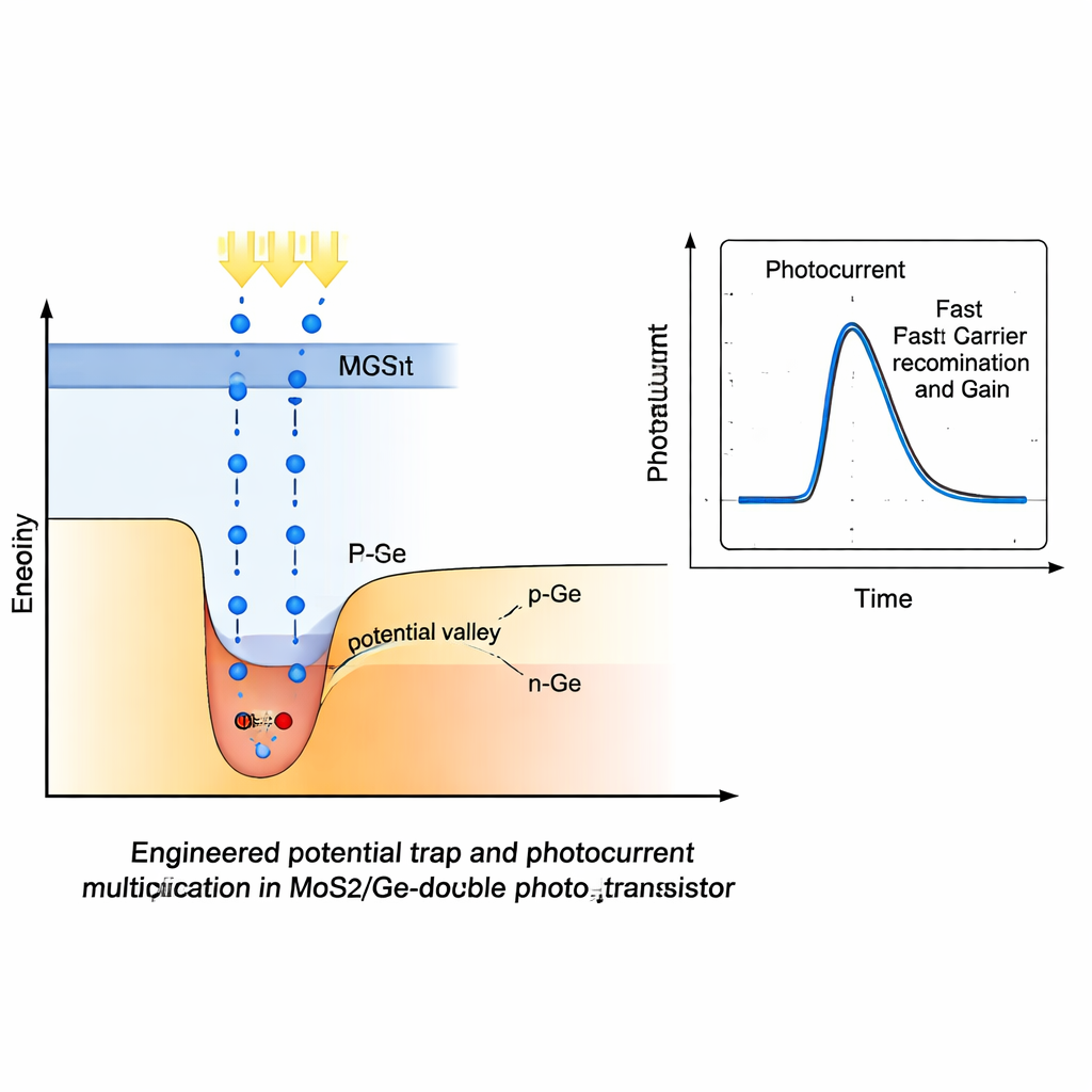
When light strikes the device, it generates pairs of electrons and holes in both MoS2 and Ge. Thanks to the way the energy levels line up across the stacked materials, most of the positively charged holes become confined in the p-type Ge base, while the negatively charged electrons are drawn out through the outer contacts. As holes pile up in the base, they lower the energy barrier that normally blocks electrons from flowing from the MoS2 emitter into the Ge. This barrier-lowering effect means that a single photo-generated hole can enable many additional electrons to flow, amplifying the electrical signal far beyond what direct light absorption alone would produce. Crucially, because this “trap” is built into the smooth energy landscape of the junctions—rather than into random defects—those stored holes disappear quickly once the light is turned off, so the device does not suffer from a long afterglow.
Fast, Bright Signals Across the Spectrum
Experiments show that this double-junction phototransistor delivers both high gain and fast response. Under blue visible light (466 nanometers), the device reaches a responsivity of about 7.6 amperes per watt—corresponding to more than twenty times as many electrons collected as photons arriving—and a maximum photocurrent gain near 29. Under SWIR light at 1550 nanometers, which is attractive for eye-safe lidar and night vision, it still achieves strong gain and responsivity around 4.7 amperes per watt. Yet the response times remain in the hundred-microsecond range for both colors, fast enough for video and rapid scanning. The authors even demonstrate simple 32×32-pixel images of a smiley-face mask under both visible and SWIR light, confirming that the sensor can form clear pictures across a broad range of wavelengths.
What This Means for Future Cameras
By deliberately engineering where and how charges are stored and released inside a tiny stacked structure of MoS2 and Ge, this work breaks a long-standing compromise in photodetectors: you no longer have to choose between speed and sensitivity. The device acts like a transistor that is turned on by light, boosting small optical signals into large, quickly changing electrical currents. Because Ge and layered materials like MoS2 can, in principle, be integrated with existing semiconductor platforms, this approach could lead to compact, relatively low-cost cameras that see both visible and SWIR light. Such sensors could improve safety in autonomous driving, enable gentler and clearer medical imaging, and make advanced infrared vision available in everyday technologies rather than just in specialized, high-end equipment.
Citation: Park, Y., Jung, M., Jeong, H.B. et al. Fast photo-carrier multiplication by engineered potential trap in MoS2/Ge double junction phototransistor. Sci Rep 16, 4885 (2026). https://doi.org/10.1038/s41598-026-35134-z
Keywords: short-wave infrared imaging, broadband photodetector, MoS2 germanium sensor, high-speed light detection, photocurrent gain