Clear Sky Science · en
Design and performance analysis of a vertically stacked gate-all-around nanosheet FET with embedded nanocavity for biosensing applications
Smaller Sensors for Earlier Warnings
Catching cancer early often depends on how quickly and accurately we can spot tiny traces of disease in blood or other body fluids. This paper explores a new type of ultrasmall electronic sensor—built with the same kind of technology used in advanced computer chips—that can detect cancer‑related molecules with far higher sensitivity than many existing devices, while using very little power.
Turning a Transistor into a Cancer Detector
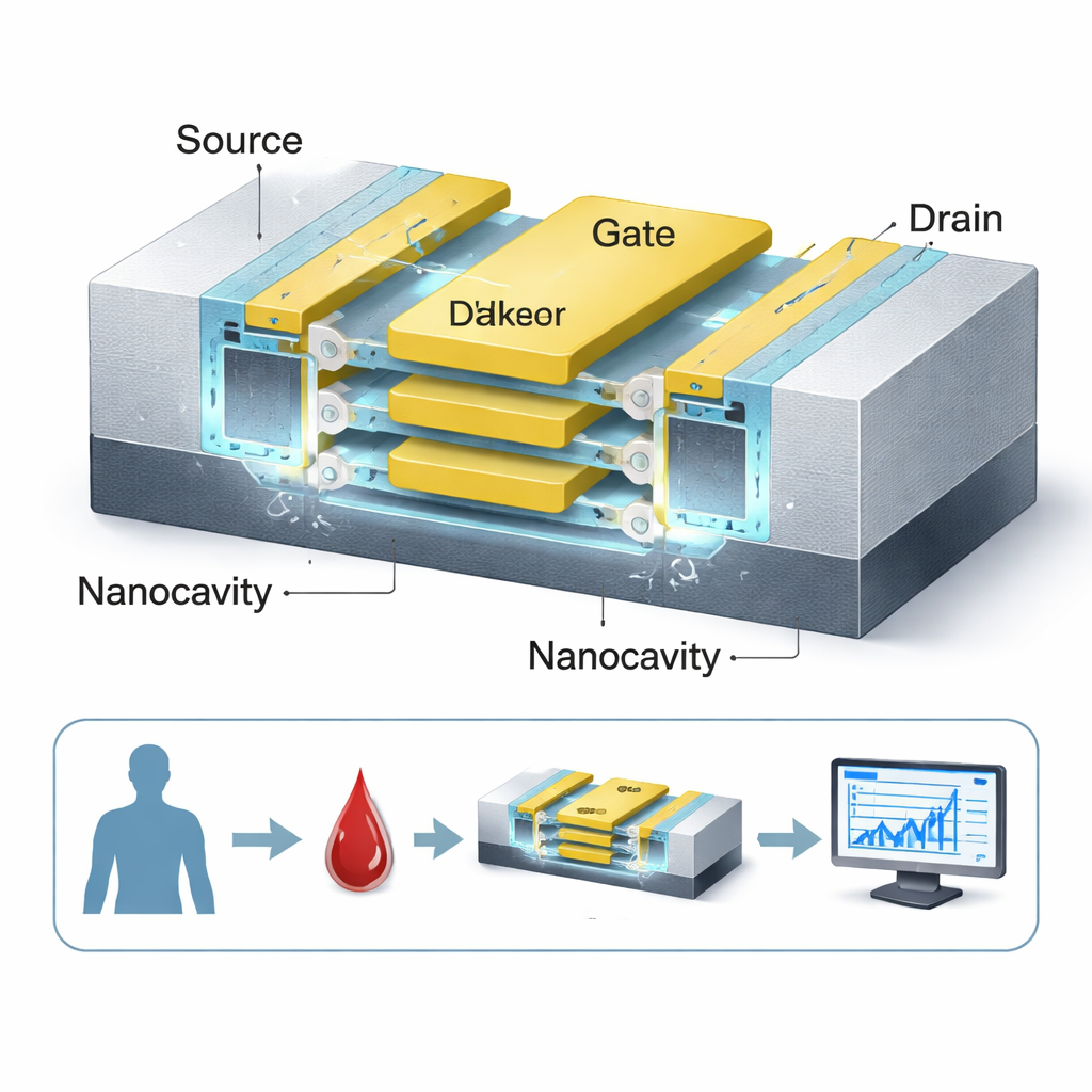
At the heart of the work is a redesigned transistor, the basic switching element in electronics. The authors start from a cutting‑edge style of device called a nanosheet FET, already being adopted by major chip makers for 3 nm processors. They repurpose it as a biosensor by carving tiny hollow regions, or nanocavities, around the insulated gate that controls current flow. When cancer‑linked biomolecules—such as cells from colorectal or kidney tumors, strands of DNA, or gelatin‑like proteins—settle into these cavities, they subtly change how electric charge moves inside the device. The transistor “feels” this change as a shift in current, turning a biochemical event into an electrical signal that can be measured.
Stacking Layers for Stronger Signals
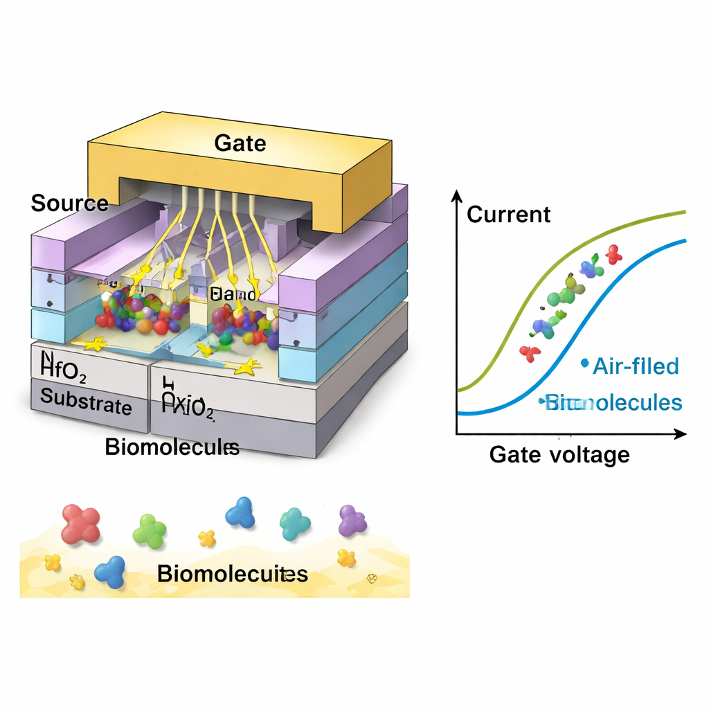
A key twist in the design is that the sensing channel is not a single wire but three ultra‑thin silicon sheets stacked vertically, all wrapped by a common gate. This gate‑all‑around structure gives the gate much tighter control over the channel than in traditional flat transistors, which sharpens the device’s on/off switching and boosts the measurable change when biomolecules are present. Two nanocavities are positioned on either side of a high‑k insulating layer (HfO₂), maximizing the region where molecules can interact with the electric field. Because the channel is “doping‑less,” meaning it avoids heavy chemical impurities, the sensor’s response is more uniform and less vulnerable to fabrication variations—an advantage for reliable medical testing.
Tuning Tiny Cavities for Maximum Response
Using detailed computer simulations (TCAD), the researchers systematically adjust the geometry of the cavities: their length, thickness, and how fully they are filled with molecules. Shorter and thinner cavities bring the gate and channel into closer electrostatic contact, raising the on‑current and reducing the so‑called subthreshold swing—a measure of how sharply the device turns on. In their optimal design, the sensor reaches a remarkably low swing of about 28 millivolts per decade, well below the 60 mV/dec limit of standard transistors. This means the device reacts strongly to very small voltage changes, a crucial trait for spotting low concentrations of biomolecules. They also show that as more of the cavity volume is occupied—or as molecules sit closer to the point where current begins—the signal grows stronger, clarifying how crowding and placement of targets affect performance.
Reading Cancer Clues in Electrical Signals
The team then explores how different types of biomolecules would look electrically. Neutral species with higher inherent permittivity (an electrical property related to how they polarize in a field) lead to larger changes in current and better sensitivity, with the strongest response at a value typical of gelatin and some dense biological tissues. Charged molecules, such as DNA or certain cell surfaces, can enhance the signal even more. In simulations, negatively charged biomolecules give the largest current shift, followed by positive charges and then neutral ones. Under optimal conditions, the device achieves current sensitivity more than 3,000 times higher than its baseline and over 9,000 for strongly negative charges—outperforming several earlier nanosheet‑based biosensors. The sensor also shows fast response times, stable operation near room temperature, and good specificity, meaning it can distinguish target molecules from similar but unwanted ones.
Toward Practical, Chip‑Level Cancer Tests
To make sure this concept is realistic, the authors outline a fabrication flow that closely follows today’s advanced chip manufacturing, using standard silicon‑on‑insulator wafers, known oxide and metal layers, and common etching steps to form the nanocavities. Because the structure stays compact and compatible with mainstream CMOS processes, it could, in principle, be integrated into dense arrays on a single chip. For a lay reader, the upshot is that this work pushes transistor‑based biosensors closer to practical lab‑on‑a‑chip devices that might one day screen for cancer markers quickly, with high sensitivity, and without the need for labels or complex chemistry, using technology very similar to that already powering modern electronics.
Citation: Prasanna, R.L., Karumuri, S.R., Sreenivasulu, V.B. et al. Design and performance analysis of a vertically stacked gate-all-around nanosheet FET with embedded nanocavity for biosensing applications. Sci Rep 16, 5508 (2026). https://doi.org/10.1038/s41598-026-35132-1
Keywords: cancer biosensor, nanosheet FET, lab-on-a-chip, nanocavity sensor, early detection