Clear Sky Science · en
High-fidelity chip delayering using green (515 nm) femtosecond lasers
Peeking Inside the Chips That Run Our World
Modern life depends on tiny semiconductor chips that quietly power aircraft, medical devices, factories, and everyday electronics. When these chips fail, or when old designs must be copied and verified, engineers need to uncover and map their hidden wiring without destroying it. This study shows how an extremely fast "green" laser can gently peel back a chip’s layers with far greater cleanliness and control than older methods, opening the door to more reliable repairs, security checks, and forensic investigations of critical hardware.
Why Opening Old Chips Matters
Many long‑lived systems—from jet engines to hospital equipment—still depend on integrated circuits whose original blueprints have been lost and whose replacement parts are no longer made. To keep these systems running, specialists must reverse engineer the chips, reconstructing their buried metal wiring so they can reproduce or evaluate the design. The same need arises in cutting‑edge manufacturing, where tiny mistakes or even hidden tampering during production can slip through and cause failures or security risks later. All of these tasks hinge on one hard problem: exposing each internal metal layer cleanly, over large areas, without blurring or erasing the features you are trying to study.
Limits of Traditional Chip Peeling
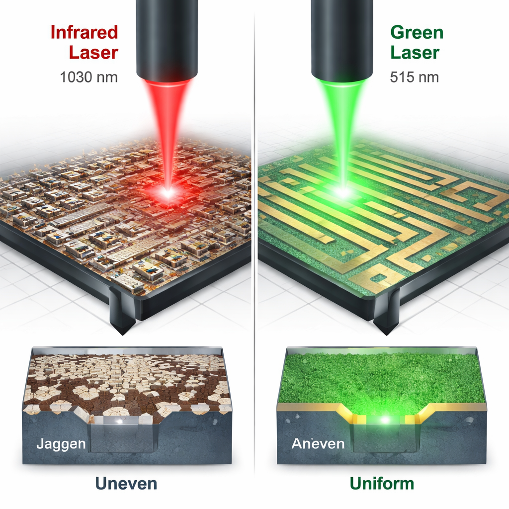
Older approaches to stripping away layers—like mechanical polishing, chemical etching, and focused ion beams—are either too rough, too slow, or too expensive to use routinely on whole chips. Mechanical and chemical methods can easily gouge or unevenly remove material, while focused ion beams offer exquisite precision only over tiny regions and at a crawl. Even non‑destructive X‑ray imaging usually lacks the sharpness needed to trace microscopic metal lines. Earlier work with ultrafast infrared lasers hinted at a better path: using extremely brief light pulses to vaporize material with less heat spread. But because different chip materials absorb infrared light very differently, this approach often produced patchy removal, leftover debris, and partially damaged wiring, which blurred the very details engineers wanted to see.
A Sharper Green Laser Scalpel
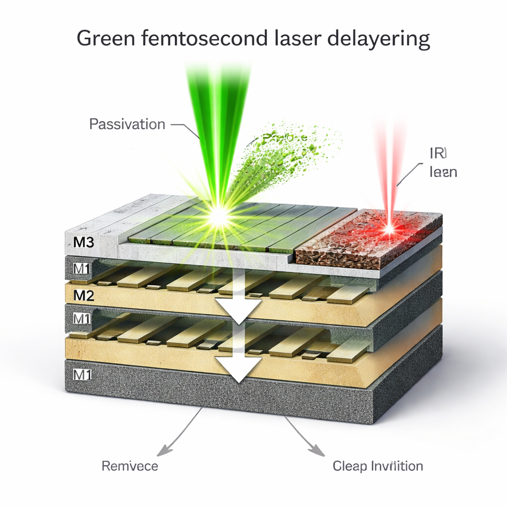
The authors tackled this challenge by switching to a green laser with pulses lasting only femtoseconds—millionths of a billionth of a second. At this shorter color, the laser’s energy couples more evenly into metals and insulating materials alike, leading to smoother removal and finer control over depth. Working on a real microprocessor with three stacked metal layers, they carefully tuned key settings such as pulse energy, repetition rate, scan speed, and pulse duration. They also recognized that not all parts of a chip look the same: some areas hold broad power lines, others dense grids of tiny connections, and still others large contact pads. By categorizing the chip into four typical region types, they could adjust their recipes so each area was cleaned without being over‑cut.
Two Ways to Use the Green Light
The team explored two main workflows. In the first, a more powerful infrared beam quickly removed bulk material, and the green laser then polished the exposed surfaces. This combination did improve cleanliness compared with infrared alone, but the repeated infrared passes tended to eat into the metal lines, subtly eroding them. In the second workflow, the green laser handled both removal and polishing from start to finish. Although this required more careful tuning, it yielded remarkably flat, low‑debris surfaces and crisp metal features across large regions, especially for the top wiring layer and much of the second layer just one micrometer below. High‑resolution confocal microscopes, electron microscopes, and elemental mapping tools all confirmed that the green‑only approach exposed the true geometry and composition of the wiring with minimal damage.
What This Means for Real‑World Chips
The study concludes that green femtosecond lasers offer a powerful and practical way to "unstack" chips layer by layer with high fidelity. Compared with relying on infrared light alone, the green approach delivers cleaner, more uniform exposure of metal layers while better preserving their shape—exactly what is needed for trustworthy reverse engineering, failure analysis, and security audits. Some especially intricate regions still pose challenges, but the authors argue that smarter parameter tuning, automated control, or pairing the laser with ultra‑fine finishing tools could push performance even further. For engineers and security experts, this technology promises a faster, more reliable window into the hidden wiring of both aging legacy components and tomorrow’s most advanced microelectronics.
Citation: Anaei, M.T.M., Maniscalco, M., Choi, H. et al. High-fidelity chip delayering using green (515 nm) femtosecond lasers. Sci Rep 16, 5495 (2026). https://doi.org/10.1038/s41598-026-35091-7
Keywords: semiconductor reverse engineering, laser chip delayering, green femtosecond laser, microchip failure analysis, integrated circuit imaging