Clear Sky Science · en
Field-tunable charge confinement in III–V layered nanowire-array superlattices
Why tiny wires and electric fields matter
Today’s fastest chips, sensors, and light-based devices increasingly rely on structures so small that electrons behave more like waves than particles. This study explores how to use simple electric fields to steer where those electrons prefer to sit inside forests of ultra-thin semiconductor “wires.” By showing that charges can be shifted, squeezed, and parked in specific layers on demand, the work points toward future electronics and photonics that can be reprogrammed after fabrication rather than fixed at the factory. 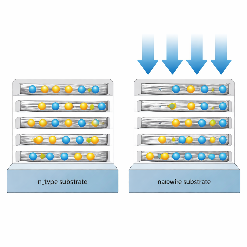
Stacks of nano-size rails for electrons
The researchers focus on a special kind of material made from gallium arsenide and aluminum gallium arsenide, both widely used in high-speed electronics and lasers. Instead of a flat film, they consider many narrow ridges—nanowires—grown side by side on a crystal surface, then repeated in vertical stacks, like several floors of train tracks for electrons. This periodic stacking forms what physicists call a superlattice, but here the pattern runs across and between separate wires rather than along a single one. Because the nanowires assemble themselves during growth, the overall structure can be created without the painstaking patterning steps used in standard chip-making.
A simplified yet realistic picture of electron motion
Directly simulating the motion and mutual repulsion of many electrons in these intricate stacks would overwhelm even powerful computers. Instead, the authors build a stripped-down but carefully calibrated model that follows two representative electrons. They assign these electrons an effective mass appropriate for gallium arsenide, confine them inside a grid of rectangular channels that mimic real nanowire dimensions, and let them interact through a “screened” force that accounts for the presence of other charges in the material. They then solve the quantum mechanical equations that describe how the electrons spread out, tunnel between neighboring wires, and respond to an applied electric field crossing the stack. 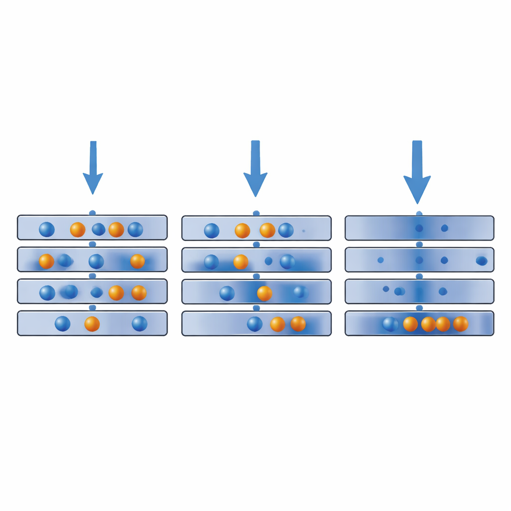
From shared highways to pinned charge layers
When there is no field applied, the electrons can tunnel between layers, forming energy ranges—called minibands—that let them move rather freely through the vertical stack. By changing basic design choices such as how wide each wire is or how thick the barriers are between layers, the team shows that these minibands can be made broader or narrower and shifted up or down in energy, much like tuning lanes on an electronic highway. Adding a transverse electric field then gradually tilts the playing field: at low strengths, energy levels barely budge, but as the field grows, the minibands shift and broaden, and the electron probability steadily drains from the upper layers to the lower ones. At strong fields, the electrons stop behaving like shared travelers in a band and instead gather into narrow charge pockets at the bottom of the structure.
When electrons push back on each other
The model also captures the fact that electrons repel one another. At low overall density, this repulsion is less well screened and becomes more important. The calculations show that even without an external field, two electrons tend to keep some distance along the length of a nanowire, creating patterns reminiscent of tiny crystalline arrangements. When a field is switched on, these interaction-driven patterns shrink and slide toward the lower layers, as the electric pull competes with the electrons’ desire to stay apart. The result is a rich set of charge layouts that can be reshaped in both the vertical and lengthwise directions simply by dialing the field strength.
Toward reprogrammable nano-optoelectronic devices
Overall, the study demonstrates that self-assembled stacks of semiconductor nanowires can act as field-tunable containers for electrons, smoothly switching between extended conduction paths and tightly localized charge layers. Because the required electric fields, dimensions, and materials already match what leading fabrication methods can deliver, these findings offer a realistic route to devices whose behavior—such as how they conduct, detect light, or store information—can be reconfigured after they are built. In everyday terms, the work shows how to turn a tiny, three-dimensional jungle gym of wires into a programmable playground for electrons.
Citation: Méndez-Camacho, R., Cruz-Hernández, E. & López-López, M. Field-tunable charge confinement in III–V layered nanowire-array superlattices. Sci Rep 16, 8021 (2026). https://doi.org/10.1038/s41598-025-34590-3
Keywords: nanowire superlattices, charge confinement, electric field control, quantum tunneling, optoelectronic devices