Clear Sky Science · en
Performance optimization of InSe-FETs using high-k dielectric materials for analog/RF applications
Faster, Smarter Electronics on a Tiny Sheet
Modern gadgets—from 5G phones to radar and medical scanners—depend on transistors that can both amplify faint signals and operate at very high speeds. This paper explores how a promising ultra-thin material, indium selenide (InSe), could be fine‑tuned to deliver stronger signal gain for future analog and radio‑frequency (RF) circuits, the kind used for wireless communication and sensing. By carefully choosing the insulating layer that sits next to the active channel in the transistor, the authors show how to boost performance while navigating an unavoidable trade‑off between power and speed. 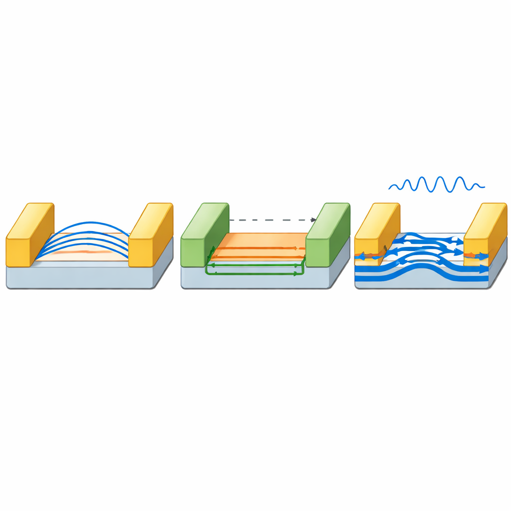
New Materials Beyond Everyday Silicon
For decades, silicon has been the workhorse of electronics, but engineers are now looking to atomically thin materials that can be peeled off in layers only a few atoms thick. These “2D” materials can be flexible, transparent, and highly efficient at carrying electric charge. Graphene was the first star of this class, but because it lacks an energy gap, it struggles in conventional on–off switching. Materials like indium selenide offer a middle ground: they keep the benefits of 2D layers while having an energy gap that lets devices switch cleanly and handle low‑power operation. Earlier studies mainly examined InSe for digital logic and light sensing; this work shifts attention to its role in analog and RF circuits, where smooth amplification and high‑frequency behavior matter more than just binary switching.
How Changing the Invisible Layer Alters Device Behavior
Every field‑effect transistor relies on a gate that controls a thin channel of charge using an insulating layer, or dielectric, in between. Here, the authors simulate InSe transistors with different dielectric materials, from a standard oxide similar to those used in silicon chips to so‑called high‑k dielectrics that store electric charge more effectively. Using detailed quantum‑level computer models, they calculate how electrons travel through a nanometer‑scale InSe ribbon when the gate voltage is varied. As the dielectric constant increases, the electric field from the gate “grasps” the channel more strongly, pulling more charge into motion and lowering the energy barrier that electrons must cross. This leads to a higher current when the device is on and a cleaner separation between on and off states, which is good news for both digital and analog use.
Turning Better Control into Stronger Signal Gain
The real focus of the study is on analog and RF figures of merit—quantities that describe how well a transistor can amplify signals and at what cost in power or bandwidth. With high‑k materials, the simulated InSe devices show nearly double the transconductance, a measure of how effectively changes in input voltage are turned into changes in output current. This, in turn, raises the intrinsic gain, which combines transconductance with how firmly the device holds its output voltage steady. The authors also examine composite measures that blend gain, speed, and efficiency—such as how much gain can be achieved at a given operating frequency or how effectively each unit of current is used to achieve amplification. In all of these, higher‑k dielectrics provide clear advantages, sometimes improving performance metrics by 70 to more than 150 percent. 
The Cost of Extra Punch: A Hit to Top Speed
There is, however, no free lunch. The same high‑k dielectric that strengthens the gate’s grip on the channel also increases the device’s capacitance, meaning it stores more charge that must be moved every time the transistor switches. While the drive current and gain improve, this extra charge slows the ultimate pace at which the transistor can operate, slightly reducing the cut‑off frequency—the point at which it no longer provides useful amplification. In the simulations, this speed metric drops by about 10 percent for the highest‑k case compared with the conventional oxide. The authors highlight this as a design trade‑off: engineers can tune the dielectric choice depending on whether strong gain, top‑end frequency, or an optimal balance between the two is most important.
What This Means for Future Wireless and Sensing Chips
In simple terms, the study shows that by swapping the thin insulating layer in an InSe transistor for a better “charge‑holding” material, engineers can build tiny switches that amplify signals much more effectively, albeit with a modest reduction in maximum speed. This makes high‑k InSe devices especially attractive for low‑voltage analog and RF circuits where clean gain and energy efficiency matter more than pushing into the absolute highest frequencies. As modeling becomes more realistic—by adding effects such as scattering and defects—and as fabrication techniques improve, such tailored 2D‑material transistors could underpin a new generation of flexible, power‑frugal communication and sensing technologies.
Citation: Ahmad, M.A., Imam, M., Mech, B.C. et al. Performance optimization of InSe-FETs using high-k dielectric materials for analog/RF applications. Sci Rep 16, 9573 (2026). https://doi.org/10.1038/s41598-025-21242-9
Keywords: indium selenide transistors, high-k dielectrics, analog RF electronics, 2D semiconductor devices, nanoelectronics simulation