Clear Sky Science · en
Imaging the sub-moiré potential using an atomic single electron transistor
Peering into the Invisible Landscape of Electrons
Every electronic device, from smartphones to quantum computers, relies on how electrons move through materials. Yet the tiny “landscapes” of electric potential that guide those electrons have mostly been invisible. This research reveals, for the first time, a direct image of such a landscape in a designer material made from stacked atom‑thin crystals. By doing so, it exposes surprises that challenge existing theory and opens a new route to visualizing some of the strangest electronic states known.
Designer Patterns in Atom-Thin Materials
When two ultra-thin crystals, like graphene and hexagonal boron nitride (hBN), are stacked with a slight twist or mismatch, they create a larger repeating pattern called a moiré lattice. This pattern acts like an artificial crystal for electrons, producing new behaviors such as unusual magnetism and exotic versions of the quantum Hall effect. In the graphene/hBN system, this engineered pattern has been central to many breakthroughs in so‑called “twistronics.” But until now, scientists could only infer the underlying electric potential landscape indirectly, from transport or optical measurements. The actual shape and strength of the moiré potential—the hills and valleys that electrons feel—had never been directly seen.
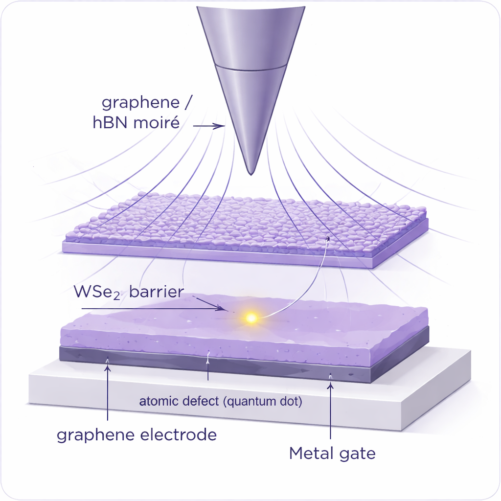
A Single Atom as an Ultra-Sensitive Meter
The authors introduce an “atomic single electron transistor” (atomic SET), a new kind of scanning probe that uses a single atomic defect as an ultra-sensitive detector of local electric potential. The defect sits inside a thin layer of a semiconductor (WSe₂) and behaves like a quantum dot: it allows electrons to tunnel one by one, and the energy at which this happens shifts in response to tiny changes in the surrounding potential. Instead of moving the defect over the sample, the team flips the usual geometry. They mount the material of interest—graphene aligned with hBN—on the tip of a quantum twisting microscope and scan it across the fixed defect. As the moiré pattern passes over the defect, it subtly “gates” the quantum dot, and by tracking the shift of its conductance peak, the researchers map the local electrostatic potential with nanometer precision.
Imaging the Moiré Landscape in Real Space
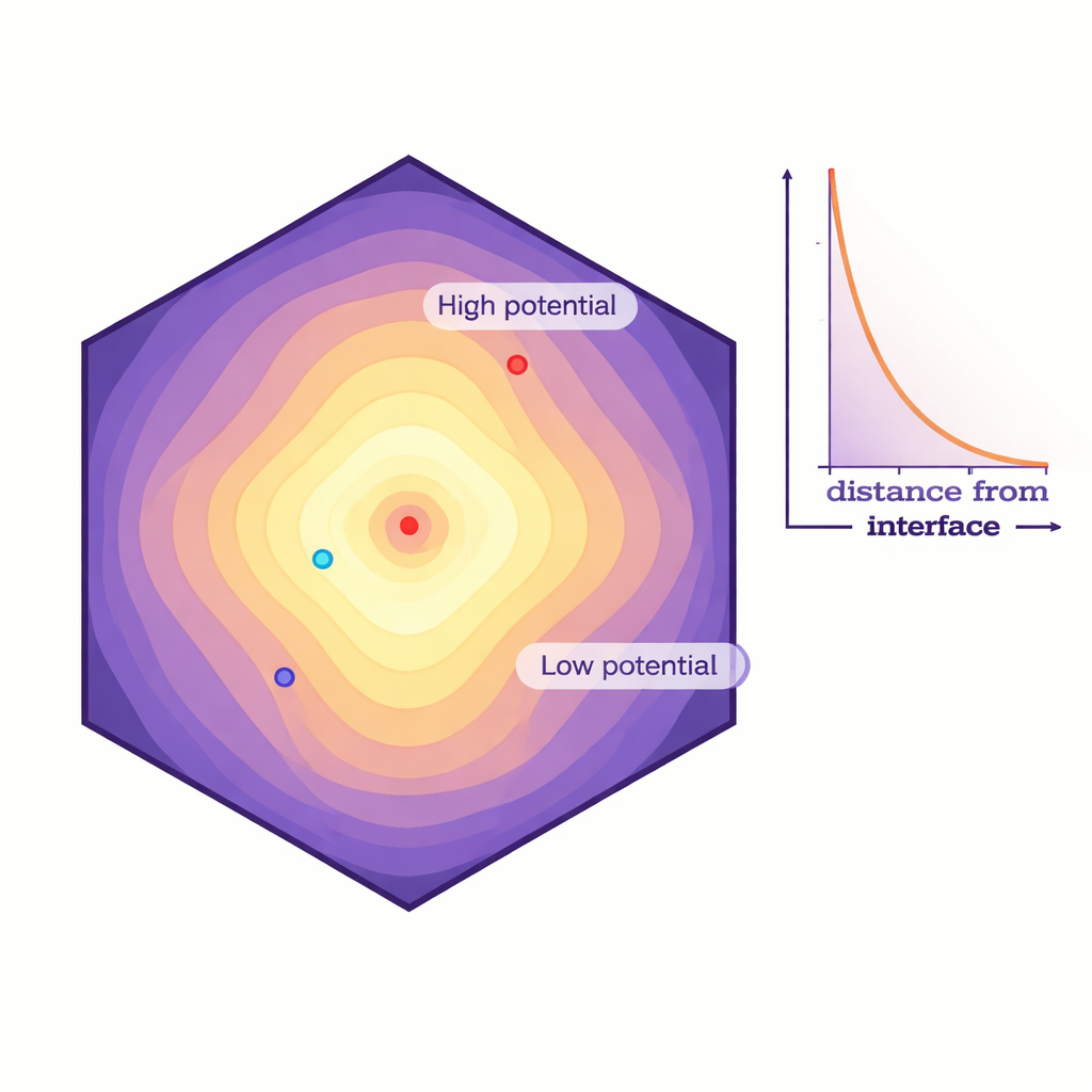
Using this atomic SET, the team obtains two- and three-dimensional maps of the potential in a single moiré cell. They find that even when there are essentially no extra electrons added to graphene (zero carrier density), the potential varies strongly—by about 60 millivolts from valley to peak. This is a substantial energy scale for electrons in such a system. The pattern has a near sixfold rotational symmetry, with a central maximum and two nearly equivalent minima separated by 60 degrees, reflecting the repeating stacking configurations of carbon atoms over boron and nitrogen atoms in hBN. Remarkably, the overall amplitude of the potential changes only weakly—by roughly 10 percent—as the electron filling of the moiré lattice is varied, meaning that the landscape is largely set by the atomic structure itself rather than by how many electrons are present.
Theory Tested, and Found Wanting
The researchers then compare their measurements with detailed theoretical models of the graphene/hBN interface. These models include contributions from how the two layers are stacked, how the graphene sheet subtly stretches and relaxes, and how electrons reorganize to screen electric fields. The various ingredients individually favor a threefold symmetry, but when combined they nearly cancel certain asymmetries, naturally producing a pattern close to the sixfold one observed in the experiment. However, the theory predicts a potential that is only about half as strong as what is actually measured. Simply assuming more strain in the material cannot fix this mismatch without ruining the observed symmetry. This discrepancy suggests that even in this “textbook” moiré system, important physical effects are still missing from current models.
Why This Matters for Future Quantum Materials
Beyond resolving a long-standing experimental challenge, the atomic SET method provides a powerful new window into quantum materials. It achieves roughly 1-nanometer spatial resolution and is sensitive to potential variations corresponding to only a few millionths of an electron’s charge at that distance. The measurements also show that the moiré potential decays quickly with distance from the interface, yet remains strong enough to influence even relatively thick stacks of graphene. Together, these capabilities will allow scientists to directly image charge order, subtle symmetry breaking, and fractionalized excitations in a wide variety of engineered quantum systems, from Wigner crystals to topological states, rather than inferring them indirectly.
Citation: Klein, D.R., Zondiner, U., Keren, A. et al. Imaging the sub-moiré potential using an atomic single electron transistor. Nature 650, 875–881 (2026). https://doi.org/10.1038/s41586-025-10085-z
Keywords: moiré materials, graphene, scanning probe, quantum dot sensor, electrostatic potential