Clear Sky Science · en
Large-scale analogue quantum simulation using atom dot arrays
Building Tiny Quantum Labs in Silicon
Many of the strangest and most useful behaviors in modern materials—like high-temperature superconductivity or exotic magnets—come from electrons strongly interacting with each other. These effects are incredibly hard to calculate, even on today’s supercomputers. This paper reports a new way to study such complex quantum behavior in the lab by building a highly controlled, silicon-based playground for electrons made from 15,000 atom-scale “quantum dots.” It is a step toward using engineered chips, rather than equations alone, to understand and design future quantum materials.
A Designer Playground for Electrons
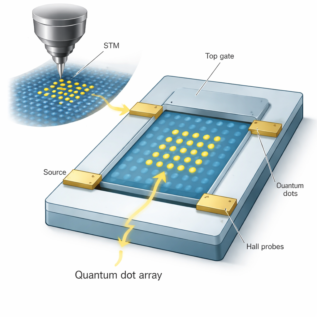
The researchers start with an ultra-clean silicon surface and use a scanning tunnelling microscope—a tool that can move and remove individual atoms—to draw patterns a few billionths of a meter across. In these patterns they implant phosphorus atoms, which donate electrons and form quantum dots: tiny islands where electrons can sit and hop between sites. By repeating this process with sub-nanometre precision, they create large, two-dimensional grids of 15,000 quantum dots arranged like points on graph paper. Because everything is defined atom by atom, they can choose not only square grids but also more exotic layouts, such as honeycomb or Lieb lattices, which mimic the crystal structures of real quantum materials.
Turning Silicon into a Quantum Testbed
To turn these delicate atomic patterns into practical devices, the team buries the quantum dot array under a thin layer of silicon, adds heavily doped silicon leads for electrical contact, and places a metal gate on top to control the overall charge. The finished structure looks like a conventional Hall bar chip used in electronics labs, but its active layer is an artificial crystal made of quantum dots instead of atoms in a natural mineral. Within this artificial crystal, key energy scales—how strongly electrons repel each other on a site, how much they feel neighbors, and how easily they tunnel between dots—can be engineered by adjusting dot size and spacing, parameters that are nearly impossible to control so flexibly in ordinary materials.
Watching a Metal Freeze into an Insulator
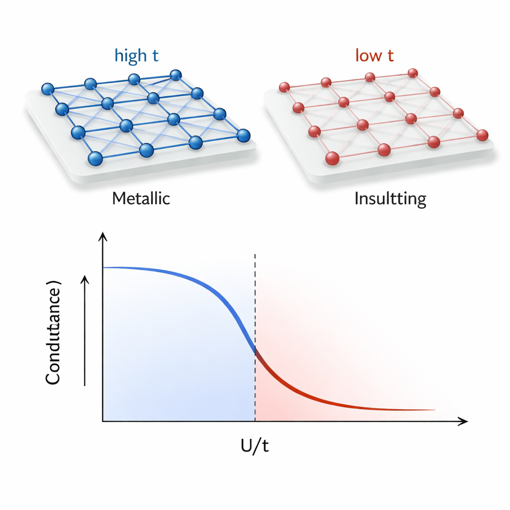
A central goal is to observe a metal–insulator transition, where a system that normally conducts electricity suddenly stops conducting as interactions or disorder increase. The authors fabricate several nearly identical arrays in which only the spacing between dots is changed. Larger spacing weakens the tunnelling between sites while leaving the local repulsion largely the same, effectively increasing the ratio of interaction energy to hopping energy. Electrical measurements at temperatures down to a few hundredths of a degree above absolute zero reveal that closely spaced arrays behave like metals, while more widely spaced ones become poor conductors and then turn strongly insulating. The critical conductance at which this transition happens matches theoretical expectations for systems where both strong interactions and randomness matter, a regime known as Mott–Anderson physics.
Probing the Hidden Quantum Mechanics
To confirm that the insulating behavior truly stems from interactions, the team studies arrays with the same spacing but different dot sizes. Smaller dots confine electrons more tightly, boosting their mutual repulsion, whereas larger dots soften it. By sweeping voltage across the device, they see clear energy gaps where charge simply cannot flow, and sharp features when electrons finally have enough energy to move—signatures of interaction-driven insulating states. Applying a magnetic field further enlarges these gaps in a way that reveals how electron spins respond collectively, providing evidence that electrons are spread over each dot as designed, rather than trapped by random defects. Temperature-dependent measurements show a switch from incoherent to coherent “co-tunnelling,” where electrons effectively borrow energy to hop across multiple dots, again in line with detailed theoretical predictions for granular quantum systems.
Hints of Rich Quantum Phases to Come
In the more conductive arrays, the team also measures the Hall coefficient, a quantity that reflects how many charge carriers participate in transport and how their motion is organized. As the temperature is lowered, one device shows a sharp, non-monotonic change in this coefficient—behavior difficult to explain by simple disorder alone and reminiscent of subtle reconstructions of the “Fermi surface,” the boundary that separates filled from empty electron states in a material. Although the authors are careful not to over-interpret these signs, they argue that their platform is now precise and large enough to explore deeper questions about correlated electrons, including how magnetism emerges, how topological states form, and whether analogues of unconventional superconductivity can be engineered on demand.
Why This Matters for Future Technologies
To a non-specialist, the main message is that the authors have built a highly tunable, atomically precise chip that behaves like an artificial quantum material whose rules they control site by site. By dialling in dot size, spacing, layout, and charge, they can watch electrons smoothly transition from freely flowing to locked in place and probe the subtle quantum mechanisms behind that change. This type of analogue quantum simulator does not replace theory or digital quantum computers, but it offers a powerful new microscope into the many-electron world. Insights gained from such engineered arrays could eventually guide the design of materials with tailor-made properties, from lossless power lines to novel quantum devices.
Citation: Donnelly, M.B., Chung, Y., Garreis, R. et al. Large-scale analogue quantum simulation using atom dot arrays. Nature 650, 574–579 (2026). https://doi.org/10.1038/s41586-025-10053-7
Keywords: quantum dot arrays, analogue quantum simulation, metal–insulator transition, strongly correlated electrons, silicon quantum devices