Clear Sky Science · en
Non-local bound states in the continuum for nanoscale alignment
Sharper Chip Making Beyond the Limits of Light
Every new generation of computer chips packs more components into less space, stacking layer upon layer of circuitry. To keep these layers working together, manufacturers must line them up with astonishing precision—down to just a few billionths of a metre. Traditional optical alignment methods are now brushing against a hard boundary: the diffraction limit, a fundamental property of light. This paper presents a clever way to sidestep that barrier by using a special kind of light-trapping effect to measure tiny misalignments far smaller than conventional optics can see.
A New Way to Line Up Chip Layers
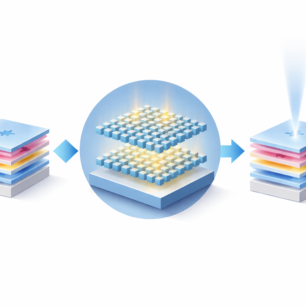
Modern chip factories already use sophisticated optical tricks—interference patterns, grating marks and image processing—to align multiple exposure steps. These approaches have boosted accuracy from micrometres to a few tens of nanometres. But as features shrink and 3D chip stacking becomes routine, even 20-nanometre errors can hurt performance and yield. The authors propose adding a new type of nanostructured pattern next to the familiar cross-shaped alignment marks on a chip. Instead of relying on sharp visual contrast, these marks harness a subtle optical phenomenon called a bound state in the continuum, or BIC, which responds exquisitely to how well two patterned layers are positioned on top of each other.
Trapping Light to Sense Tiny Shifts
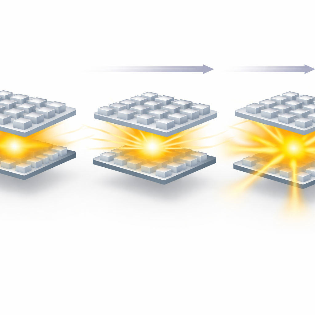
A BIC can be thought of as a light wave that becomes perfectly trapped inside a structure, even though it lives in the same range of energies as freely propagating light. In this trapped state, light does not leak out, so it produces no obvious resonance signal in a transmission spectrum. The researchers design a “meta-device” made of two layers of tiny square polymer pillars, each layer arranged in a regular hexagonal grid and separated by thin film layers on a glass substrate. When the top and bottom nanopillar arrays are exactly aligned, the structure’s symmetry protects the trapped state and the light remains hidden from the outside world, corresponding to an effectively infinite quality factor, or Q.
Turning Perfect Traps into Useful Signals
The trick is to use deliberate misalignment as a tuning knob. When the upper layer of nanopillars is shifted sideways by a small distance relative to the lower layer, the vertical symmetry of the system is broken. This disturbance converts the ideal BIC into a quasi-BIC: light is still mainly confined but now leaks out a little, creating a very sharp resonance peak in the transmitted light spectrum around a wavelength of about 590 nanometres (in the orange part of the spectrum). In simulations, and then in real fabricated samples made with nanoimprint lithography, the team systematically varies this displacement, labelled D, and tracks how the resonance changes. As D grows from zero to a few tens of nanometres and beyond, the once-infinite Q factor falls to finite values—about 200, 120 and 66 for displacements of 30, 40 and 110 nanometres, respectively—while a clear resonance feature appears and broadens.
From Laboratory Measurements to Factory Tools
Because the resonance quality is so sensitive to the relative position of the two nanopillar layers, the Q factor itself becomes a precise ruler for nanoscale alignment. Crucially, this method is not limited by the diffraction of light in the way that imaging-based techniques are. Instead of trying to resolve ever-smaller details directly, it reads out tiny displacements indirectly through changes in the resonance’s sharpness. The authors show that processing imperfections—such as roughness, slight dimensional errors or material absorption—do limit how high Q can get, but careful design choices and improved fabrication can push performance further. The double-layer nanopillar structures can be produced by standard nanoimprint steps and placed alongside existing lithography marks, making the approach compatible with current semiconductor manufacturing workflows.
What This Means for Future Chips
In essence, the study demonstrates that carefully engineered light-trapping states in nanoscale structures can act as ultra-sensitive alignment sensors. By watching how a silent, perfectly trapped light mode turns into a loud, sharp resonance as two patterned layers slip out of alignment, chip makers gain a new, physics-based handle on positioning accuracy well beyond conventional optical limits. This strategy could support more reliable, densely stacked chips and help extend the scaling of semiconductor technology into regimes where traditional alignment tools can no longer keep up.
Citation: Zhang, J.C., Tsai, D.P. & Pang, S.W. Non-local bound states in the continuum for nanoscale alignment. Nat. Photon. 20, 296–300 (2026). https://doi.org/10.1038/s41566-026-01847-w
Keywords: semiconductor lithography, nano-alignment, metasurfaces, bound states in the continuum, chip manufacturing