Clear Sky Science · en
Twisted atomic magnetic tunnel junctions with multiple nonvolatile states
Storing More Than Just Zeros and Ones
Today’s digital devices largely think in black and white: each tiny memory element holds either a zero or a one. This paper explores a way to pack more than two stable values into a single, ultra‑small magnetic device made from sheets of atoms. By carefully twisting these atom‑thin magnetic layers, the researchers show that one junction can reliably hold multiple distinct states without power, hinting at denser memory, new kinds of computing, and devices that approach the ultimate limits of miniaturization.
From Classic Magnetic Bits to Atomic Stacks
Magnetic tunnel junctions are already at the heart of modern magnetic memory and read heads in hard disks. In a conventional junction, two magnetic metal layers are separated by an extremely thin insulating barrier. Electrons can “tunnel” through this barrier more easily when the magnetizations in the two layers point in the same direction than when they point in opposite directions, giving two resistance levels that encode zero and one. This design has proved robust and scalable, but it is still built from relatively thick, imperfect oxide barriers and is fundamentally limited to just two stable states.
Why Twisted Atomic Layers Change the Game
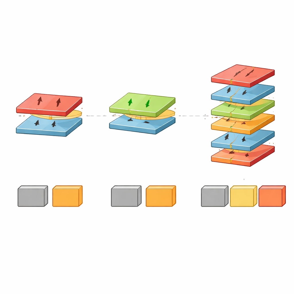
The team turns to a material called CrSBr, a semiconductor that is magnetic even when shaved down to a single atomic layer. In its natural form, two such layers couple so that their internal magnets line up within each sheet but oppose each other between sheets. When used as a barrier between conducting contacts, this bilayer already acts as an “atomic” tunnel junction. The key insight here is that rotating one CrSBr layer relative to another — creating a twisted interface — largely breaks the usual strong coupling between layers. Each twisted boundary can then support two different, stable alignments of the magnetic moments, which translate into two distinct conductance states even when no external magnetic field is applied.
Building Devices with Two and Four Stable Levels
First, the researchers stack one CrSBr monolayer on top of a natural CrSBr bilayer, forming a three‑layer structure with a single twisted interface. The bilayer beneath remains strongly locked into an antiparallel pattern, acting like a rigid reference, while the twisted interface above can settle into either a quasi‑parallel or quasi‑antiparallel arrangement. Careful magnetic‑field sweeps show that the current through this atomic‑scale junction can reproducibly switch between two zero‑field levels, with changes in resistance that can reach several hundred percent in optimized devices. Because the underlying bilayer provides strong “pinning,” these two states are unusually stable over many cycles and across a wide range of field directions.
Turning One Twisted Interface into a Multi‑Level Element
The authors then extend the design by adding a second CrSBr monolayer beneath the bilayer, creating a four‑layer stack with two twisted interfaces: monolayer/bilayer/monolayer. Now, both the top and bottom monolayers can independently adopt one of two orientations relative to the central bilayer. In combination, that yields four distinct magnetic configurations, each producing a different tunneling current at zero field. Experiments at very low temperatures show four well‑separated, reproducible current levels. By steering the direction and strength of modest magnetic fields, the team demonstrates that any one of these four states can be converted into any other, either directly or through sequences of switching steps, effectively realizing a controllable four‑level memory cell in a single atomic junction.
Toward Richer Magnetic Memory and Computing
Beyond these specific stacks, the authors show that similar ideas work when all layers are antiferromagnetic, yielding three nonvolatile levels in a device made from three twisted bilayers. Together, the results prove that simply adding twisted interfaces inside van der Waals magnetic materials can multiply the number of stable resistance states available in a single junction. For a layperson, this means a path toward memory elements that store several values instead of just zero or one, in devices only a few atoms thick. Such multi‑level, ultra‑thin magnetic tunnel junctions could one day pack far more information into the same area and enable new kinds of brain‑inspired or energy‑efficient computing architectures.
Citation: Chen, Y., Samanta, K., Healey, A.J. et al. Twisted atomic magnetic tunnel junctions with multiple nonvolatile states. Nat Commun 17, 2439 (2026). https://doi.org/10.1038/s41467-026-70239-z
Keywords: magnetic tunnel junctions, twisted 2D magnets, multi-level memory, CrSBr, spintronics