Clear Sky Science · en
Wafer-scale integration of single nanodiamonds via electrostatic-trapping
Turning Tiny Diamonds into Big Technology
Imagine shrinking parts of a quantum computer or a medical imaging device down to the size of a grain of dust. That is the promise of nanodiamonds—tiny crystals of diamond that can host special atomic defects acting like ultra-sensitive sensors and light sources. This paper shows a practical way to place vast numbers of individual nanodiamonds neatly and quickly onto computer-chip-style surfaces, a key step toward turning lab demonstrations into real-world quantum technologies.
Why Tiny Diamonds Matter
Diamonds are famous for their hardness and sparkle, but at the nanoscale they offer something even more valuable: they can host quantum “defects,” such as nitrogen-vacancy centers, that behave like single, controllable atoms. These nanodiamonds can emit single photons, sense magnetic and electric fields, and work inside living tissue, making them promising building blocks for quantum sensing, imaging, and communication. To move from one-off experiments to useful devices, engineers need to arrange single nanodiamonds precisely on chips and photonic circuits, in regular arrays that can be manufactured on an industrial scale.
The Challenge of Herding Nanodiamonds
Positioning nanodiamonds is surprisingly difficult. Unlike perfectly round nanoparticles, nanodiamonds vary in size, shape, and surface chemistry, which makes them hard to control. Existing methods—such as template-based self-assembly, intricate scanning-probe placement, or 3D printing—can create ordered patterns, but usually only over tiny areas and with low throughput. They are often slow, expensive, and incompatible with the standard CMOS processes used to fabricate modern electronics. The field has been missing a method that is simple, fast, and scalable from a few micrometers up to full wafers.
A Gentle Trap Built from Electric Charges
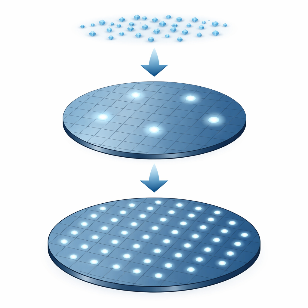
The authors introduce an electrostatic-trapping technique that acts like a silent, invisible funnel for negatively charged nanodiamonds suspended in water. They start with a silicon wafer and chemically treat its surface so that the bottoms of microscopic circular holes carry positive charges, while a photoresist layer forming the hole walls remains slightly negative. When a droplet of nanodiamond solution flows across this patterned surface, the electric field inside each hole takes on an hourglass-like shape. This field naturally steers a single, negatively charged nanodiamond down toward the center of the hole bottom, while discouraging additional particles from crowding in. After a brief incubation, the liquid is removed and the photoresist template is stripped away, leaving single nanodiamonds anchored at well-defined positions.

From Single Traps to Full Wafers
By tuning the geometry of the holes and the timing of the process, the researchers show they can reliably load one nanodiamond per site across large arrays. Experiments reveal that the key design knob is the hole diameter: small holes favor the trapping of single particles with high accuracy, while larger holes permit multiple nanodiamonds to settle. Numerical simulations of how the electric potential varies inside the holes match the experimental observations, pinpointing a narrow region—the waist of the “hourglass”—where the trapping is strongest. Using standard photolithography on 8-inch wafers, the team achieves arrays where about 82.5% of all sites contain exactly one nanodiamond, the highest combination of yield and patterned area reported so far for this kind of system.
Ready for Real Chips and Devices
Crucially, this trapping method fits comfortably into existing semiconductor manufacturing workflows. The team demonstrates precise placement of nanodiamonds on silicon waveguides, gallium nitride pillars, and gold microwave antennas—structures commonly used in photonic and microwave quantum devices. The nanodiamonds stay in place even after high-temperature processing, which is important for building complex circuits around them. Because the approach relies only on charge patterns and hole geometry, it can in principle be extended to other nanoparticles and to even larger wafers used in industry.
What This Means for Future Technologies
Put in everyday terms, the authors have developed a scalable way to “sprinkle and snap” tiny quantum-ready diamonds into orderly positions across an entire chip, using nothing more exotic than shaped holes and electric forces. This bridges a long-standing gap between small-scale laboratory placement techniques and the demands of industrial manufacturing. By making it easier to integrate single nanodiamonds wherever they are needed, this work could speed up the development of practical quantum sensors, imaging probes, and communication components that one day might sit inside medical instruments, smartphones, or data centers.
Citation: Jing, J., Wang, Y., Wang, Z. et al. Wafer-scale integration of single nanodiamonds via electrostatic-trapping. Nat Commun 17, 2636 (2026). https://doi.org/10.1038/s41467-026-69590-y
Keywords: nanodiamonds, quantum devices, electrostatic trapping, CMOS integration, nanophotonics