Clear Sky Science · en
Extreme optical nonlinearities unveiled by ultrafast laser filamentation in semiconductors
Lighting up the heart of electronic materials
Modern electronics and photonics increasingly rely on three-dimensional structures carved directly inside semiconductor crystals such as silicon, germanium, and gallium arsenide. Ultrafast lasers—firing pulses lasting trillionths to quadrillionths of a second—seem like ideal tools for this kind of precise, contactless sculpting. Yet, paradoxically, these same materials possess powerful “self-protection” mechanisms that spread out the laser’s energy and prevent permanent internal changes. This study uncovers how that self-protection works in detail, and reveals practical ways to work with, rather than against, the physics to better control light and matter at extreme intensities.
How intense light behaves inside semiconductors
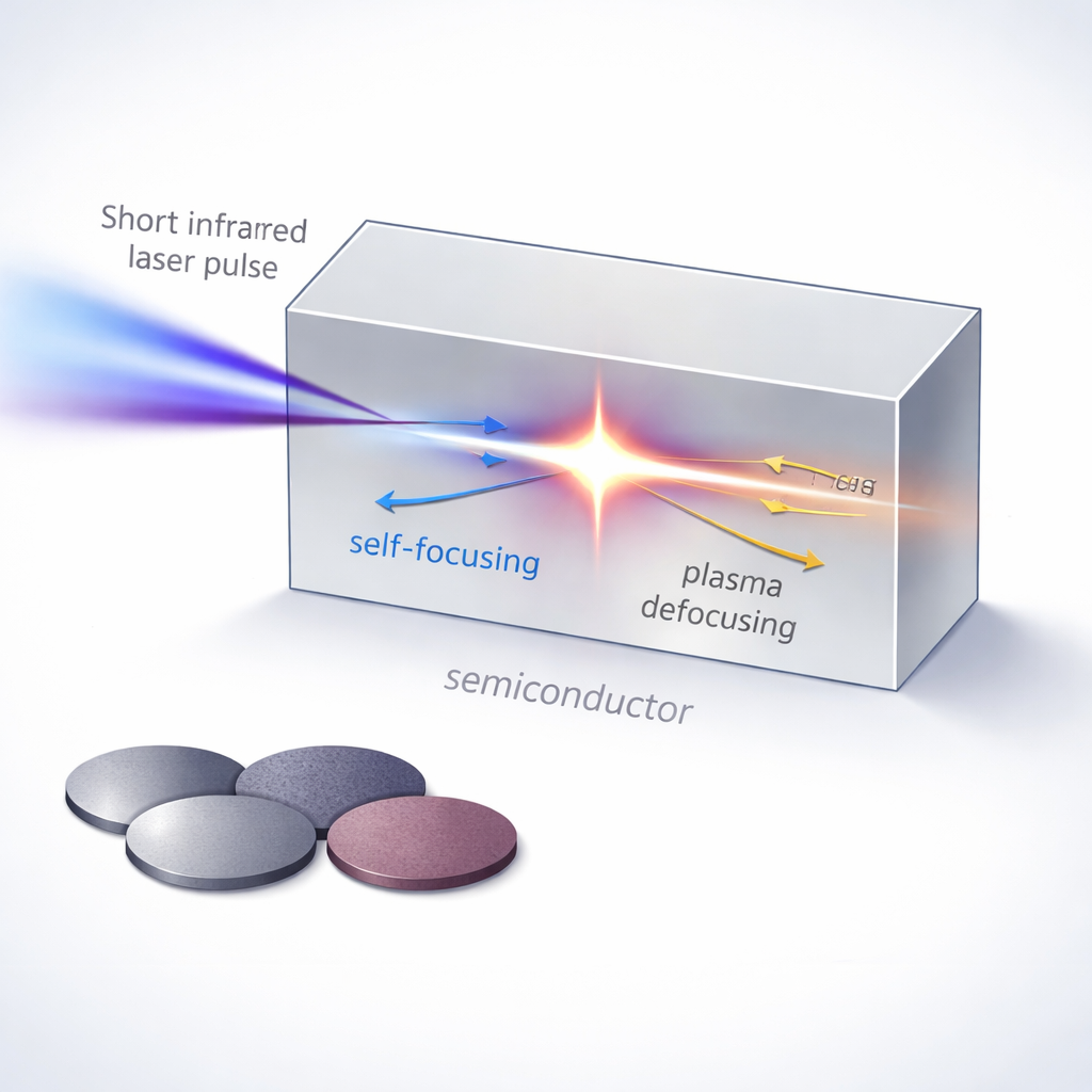
When a very strong, ultrashort laser pulse travels through a transparent material, it does not simply focus like a flashlight beam through a lens. Instead, it can form a narrow, self-guided channel of light known as a filament. This filament appears when two opposing effects balance each other: the material’s tendency to focus the beam (due to a property called the optical Kerr effect) and the tendency of laser-created charged particles to defocus it. In gases and wide-bandgap crystals, such filaments have been widely studied and even used to guide lightning or generate broad “white light.” In common semiconductors, however, the same physics has been less understood and, in practice, often ruins attempts to write sharp features deep inside the material by smearing the energy over a long path.
Seeing the energy trail in three dimensions
The authors investigated four technologically important semiconductors—silicon (Si), germanium (Ge), indium phosphide (InP), and gallium arsenide (GaAs)—all of which strongly bend and absorb light at the infrared wavelength they used. They developed a kind of optical tomography called nonlinear propagation imaging to directly map, in three dimensions, how much laser energy each tiny region inside the crystal receives. By carefully staying just below the level where the material would be permanently damaged, they could treat the glowing path of the filament as a built-in probe. As the incoming pulse energy increased, the recorded shapes evolved in a repeatable sequence: from a simple “grain of rice” focus, to a distorted “egg,” to an “angel” with wings of prefocal absorption, and finally to a “pearl necklace” of multiple bright spots. This universal progression appeared in all four semiconductors, showing that filamentation is the rule rather than the exception.
Hidden extremes in material response
From these 3D maps, the team extracted key numbers that describe how the materials react to intense light. They measured the maximum internal fluence (energy per area), the laser power at which nonlinear effects become important, and how strongly the material absorbs multiple photons at once. They repeated the experiments for pulse durations ranging from 275 femtoseconds to 25 picoseconds. Surprisingly, the peak fluence inside the material increased only up to a certain limit and then saturated, a consequence of “intensity clamping” by filamentation. Even more striking, the effective nonlinear coefficients they deduced were orders of magnitude larger than values commonly quoted from low-intensity measurements. This means that under strong excitation, the material’s response is dominated by dense plasmas of free carriers, and traditional, weak-field measurements dramatically underestimate what actually happens in real processing conditions.
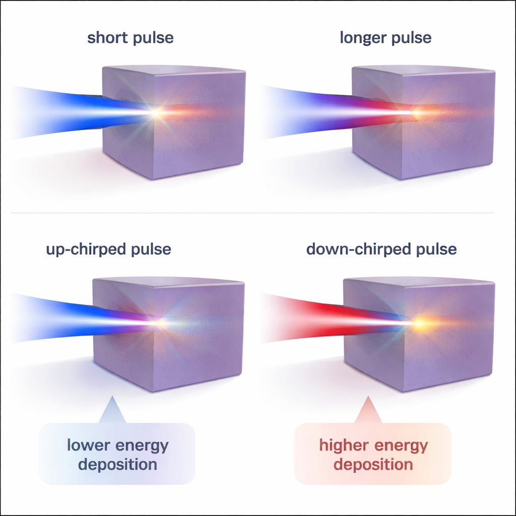
Tuning the pulse to tame the filament
Armed with this deeper understanding, the researchers explored how to deliberately reshape the laser pulses to deposit more energy where it is needed. They tested three knobs: pulse duration, temporal ordering of colors (known as chirp), and wavelength, which determines whether two, three, or more photons must combine to excite electrons. Longer pulses generally produced higher peak fluence inside the crystal and made energy deposition more localized. Down-chirped pulses—where blue spectral components arrive before red ones—enhanced the buildup of free carriers and increased peak fluence compared with up-chirped pulses of the same duration. Most importantly, using wavelengths that require higher-order multi-photon absorption significantly raised the achievable peak fluence while reducing unwanted absorption before the focus. Under these conditions, the laser can finally overcome the self-protective spreading and reach modification thresholds inside the bulk.
Turning a limitation into a design tool
For non-specialists, the takeaway is that semiconductors possess an intrinsic “immune system” against extreme light: they reshape and limit intense laser beams through filamentation. This study not only confirms that this behavior is universal across key semiconductor families, but also shows how to quantify it and, crucially, how to outsmart it. By choosing longer pulses, tailoring the chirp, and especially using longer wavelengths that trigger higher-order absorption, engineers can more effectively concentrate energy beneath a chip’s surface. These insights open the door to more reliable 3D laser writing of photonic circuits, secure microelectronics features, and advanced light sources spanning from terahertz waves to high harmonics—all built directly inside the very materials that currently resist such modifications.
Citation: Chambonneau, M., Blothe, M., Fedorov, V.Y. et al. Extreme optical nonlinearities unveiled by ultrafast laser filamentation in semiconductors. Nat Commun 17, 1701 (2026). https://doi.org/10.1038/s41467-026-69530-w
Keywords: ultrafast laser filamentation, semiconductors, nonlinear optics, laser material processing, pulse shaping