Clear Sky Science · en
Enhancing electrical conductivity by defects in metals
Turning Flaws into an Advantage
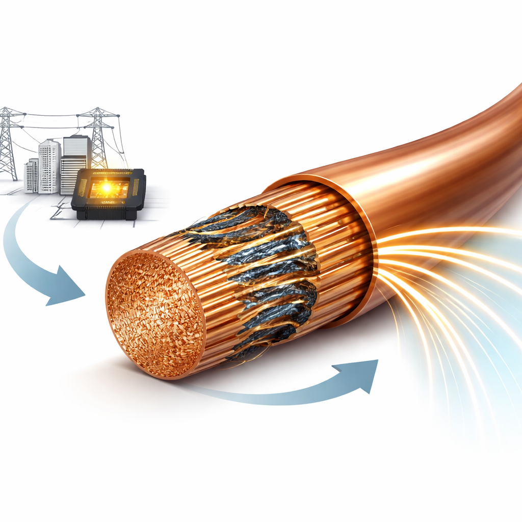
Modern life depends on moving electricity efficiently, from data rushing through chips to power flowing across cities. For more than a century, engineers have tried to make metal wires purer and smoother, because tiny flaws inside metals are known to get in the way of electrons. This study turns that long‑held belief upside down. By carefully designing and loading a metal with a special kind of internal disorder, the researchers show that copper wires can carry electricity even better than today’s best standards—without exotic conditions or expensive materials.
Why Better Wires Matter
Every electronic device loses some energy as heat when current flows. In ultra‑dense computer chips and long‑distance power lines, even small improvements in conductivity can translate into faster signals, lower error rates, and reduced power consumption. Pure copper has been the workhorse for over a hundred years, and the International Annealed Copper Standard (IACS) set its benchmark conductivity at 100%. Despite heroic efforts in purification and crystal perfection, only modest gains have been achieved since then. Even applying enormous pressures—far beyond what cables or chips ever experience—barely nudges copper’s performance. This has led to a simple rule of thumb: defects and grain boundaries are bad for conductivity and should be removed whenever possible.
Rethinking Defects Inside Copper
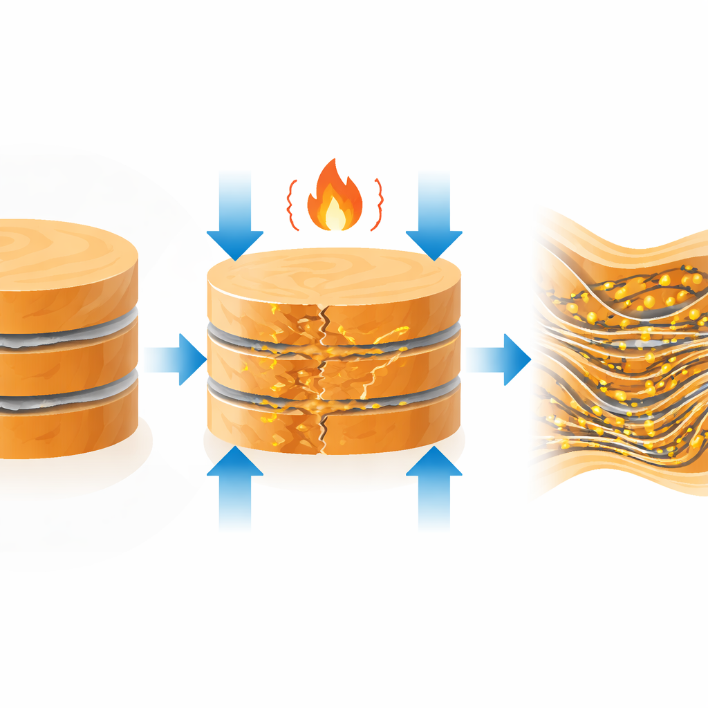
The authors challenge this rule by engineering copper that is full of interfaces yet conducts better than pristine copper. They start with thin copper foils on which a trace amount of graphene—a one‑atom‑thick form of carbon—is grown along the internal boundaries. These foils are stacked, hot‑pressed into a bulk piece, then squeezed and drawn into fine wires through many mechanical steps. Throughout this process the graphene, sitting along the copper grain boundaries, acts like a skeletal framework. It allows the material to be deformed heavily without breaking, while also slicing the copper grains down to nanoscale thickness. A final heat treatment locks in a nanolayered structure made of copper lamellae separated by graphene‑lined boundaries.
Hidden Stresses that Boost Flow
At first glance, this dense network of boundaries should make conduction worse. Instead, after annealing, the electrical conductivity of the graphene–copper wires jumps to more than 110% IACS—higher than the best single‑crystal copper and even outperforming silver when strength, weight, and cost are considered together. Microscopy and X‑ray measurements reveal why. During cooling from high temperature, copper and graphene expand and contract in different ways. Because graphene hardly expands in its plane and copper expands more, intense compressive stresses build up near their interfaces. These stresses distort the copper lattice by several percent locally, creating thin “distorted nanolayers” at the boundaries. Rather than acting as roadblocks, these strained regions become highly conductive channels that thread through the wire.
How Distortion Tames Vibrations
On the atomic scale, electrons in metals are scattered not just by impurities but also by vibrations of the lattice known as phonons. The strength of this electron‑phonon interaction is a key factor limiting conductivity. Using quantum‑mechanical calculations, the team shows that compressing copper’s lattice weakens this interaction: as strain increases, the calculated coupling constant drops significantly, and the phonon spectrum shifts in a way that reduces how strongly electrons are jostled. Their estimates indicate that the internal stresses around the graphene interfaces are equivalent to squeezing copper with tens of gigapascals of pressure—far more than is practical to apply from the outside. Yet here, that “giant pressure” is stored inside the wire itself. Measurements of how the resistivity changes with temperature support this picture: after annealing, the wires exhibit signs of stronger static disorder but a noticeably reduced contribution from thermal vibrations, consistent with suppressed electron‑phonon scattering.
Stronger, Lighter, and More Conductive
Beyond conductivity, the engineered copper wires also gain mechanical strength and maintain a relatively low density, thanks to the nanoscale grain refinement and the reinforcing graphene. This is particularly appealing because strengthening metals usually comes at the cost of worse electrical performance. The authors show that their graphene‑assisted copper breaks this trade‑off: it is stronger than conventional copper and silver, yet conducts electricity better than either, while remaining much cheaper than silver. The underlying strategy is broadly applicable: any system where an ultrathin, stiff layer can be embedded at metal boundaries could, in principle, store similar internal stresses and reshape how electrons move.
What This Means for Future Technology
The central lesson of this work is that defects and boundaries in metals are not always enemies of conductivity. When carefully arranged and placed under built‑in stress, they can reshape lattice vibrations in ways that make it easier, not harder, for electrons to flow. By turning internal strain into a permanent feature rather than relying on external pressure, the researchers demonstrate copper conductors that exceed historical limits under everyday conditions. This approach could inspire new generations of high‑performance wires and interconnects for power grids, communication networks, and advanced electronics—where invisible, stress‑tuned layers quietly help electricity glide with less resistance.
Citation: Zhang, X., Xiong, DB., Zhang, Y. et al. Enhancing electrical conductivity by defects in metals. Nat Commun 17, 2513 (2026). https://doi.org/10.1038/s41467-026-69357-5
Keywords: copper conductivity, graphene composites, nanostructured metals, electron phonon coupling, high performance wires