Clear Sky Science · en
Neuromorphic photonic computing with an electro-optic analog memory
Why Faster, Leaner AI Brains Matter
Today’s artificial intelligence runs on power-hungry computer chips that constantly shuttle data back and forth between memory and processors. This traffic jam wastes energy and slows things down, especially as AI models grow larger and more complex. The research in this paper introduces a new kind of light-based computing circuit with built‑in analog memory, designed to slash that data movement and make future AI hardware both faster and far more energy‑efficient.
Light as a New Way to Calculate
Instead of relying only on electrons in metal wires, neuromorphic photonic processors use pulses of light to carry and combine information, mimicking how signals flow through networks of neurons. Light can travel in many colors at once through the same pathway, allowing massive parallelism and extremely low delay. This makes photonic chips attractive for the heavy “multiply and add” operations that dominate neural networks. However, most existing photonic processors use fixed “weights” that must be trained elsewhere on digital hardware, then copied in. That limits how adaptable they are and still leaves a large burden on conventional memory and conversion circuits.
Bringing Memory Next to the Light
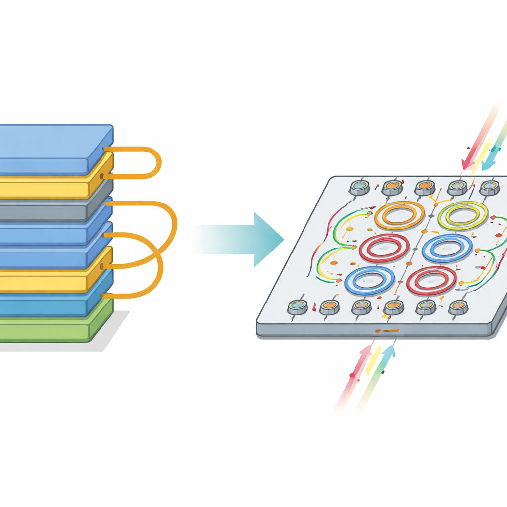
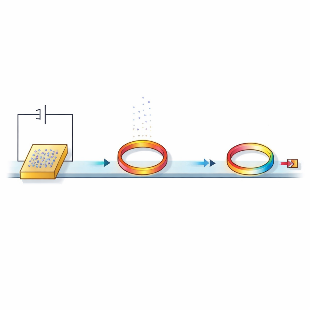
The authors tackle this by adding a simple, foundry‑friendly analog memory directly beside each tiny optical device that represents a neural network weight. Their key building block is a dynamic electro‑optic analog memory (DEOAM): an ordinary capacitor connected to a microscopic ring of silicon that guides light in a loop. A small stored voltage on the capacitor slightly shifts how the ring interacts with passing light, effectively setting the strength of a neural connection. Because the capacitor can hold this voltage for a short time, specialized digital‑to‑analog converters no longer need to drive each ring continuously. Instead, a much smaller set of converters can update many rings in sequence, while the analog memory keeps the programmed values in place.
How the Prototype Chip Works
The team fabricated a neuromorphic photonic circuit in a commercial 90‑nanometer silicon platform, combining standard electronics and nanophotonics on one chip. They built an array of ring resonators, each paired with its own capacitive memory cell, plus simple switches to write, hold, or reset the stored voltages. When a voltage is written, the ring’s response to laser light changes; when the write circuit disconnects, the capacitor keeps the voltage, and the light still “sees” the programmed weight until the charge gradually leaks away. The researchers measured key properties: the memory can be written in tens of nanoseconds, retains usable information for around a thousandth of a second, and offers roughly five bits of analog precision. Light traverses the optical paths in picoseconds, so computation itself is extremely fast compared with the time the memory values remain valid.
Testing with a Realistic Neural Network
To understand what these hardware limits mean for practical AI, the authors simulated how such a weight bank would behave inside a small image‑recognition network trained on handwritten digits from the MNIST dataset. They mapped a three‑layer network—784 inputs, 50 hidden neurons, and 10 outputs—onto realistic arrays of rings and analog memories, including noise, limited precision, finite retention, and other imperfections. The study shows that with at least about four control bits during inference, and more during full on‑chip training, the system can still reach over 95 percent classification accuracy. They also found that as long as the memory’s retention time is at least 100 times longer than the time it takes for one input to pass through the network, accuracy remains above 90 percent even though the weights slowly “leak.” In other words, a modestly short‑lived, leaky analog memory can still be very useful when the photonic computation is so fast.
Energy Savings and Design Trade‑Offs
A central benefit of DEOAM is the drastic reduction in the number of digital‑to‑analog converters. In conventional designs, every optical weight needs its own converter, so the count grows with the square of the network size. With DEOAM, converters are shared across rows or columns, and the count grows only linearly. Using real measurements from their prototype and published data for standard memory and converter circuits, the authors estimate that such an integrated analog‑memory photonic architecture can cut power use by more than a factor of 26 compared with traditional SRAM‑plus‑converter schemes. They also analyze how noise, batch size during training, and the need for periodic refreshes of the analog memory affect overall performance, outlining practical design rules for future large‑scale systems.
What This Means for Future AI Chips
For non‑specialists, the main message is that this work shows a realistic path toward AI hardware that is both extremely fast and dramatically more energy‑efficient, by letting light do the math while simple analog memories hold the settings in place. Even though these memories slowly fade, the network can tolerate and even exploit this “forgetfulness” as a form of regularization, helping avoid overfitting. By weaving memory directly into the optical fabric of the chip and sharply reducing expensive conversion steps, neuromorphic photonic processors like this could power future AI systems that learn on the fly, adapt to changing conditions, and operate at high speed without the massive energy bills of today’s data centers.
Citation: Lam, S., Khaled, A., Bilodeau, S. et al. Neuromorphic photonic computing with an electro-optic analog memory. Nat Commun 17, 2472 (2026). https://doi.org/10.1038/s41467-026-69084-x
Keywords: neuromorphic photonics, analog memory, optical computing, energy-efficient AI, silicon photonics