Clear Sky Science · en
van der Waals grain boundaries with inert electrical behaviors in inorganic molecular dielectric film
Why this tiny material matters
Modern electronics depend on ultrathin insulating layers that keep electric currents precisely where engineers want them. As chips shrink and two-dimensional (2D) materials emerge, finding insulators that are both robust and compatible with large-scale manufacturing has become a major challenge. This study explores a surprising kind of insulation made from a molecular crystal of antimony trioxide (Sb2O3) and uncovers why it works so well, even when it is full of tiny crystal grains that would normally ruin performance.
Cracks inside crystals that should cause trouble
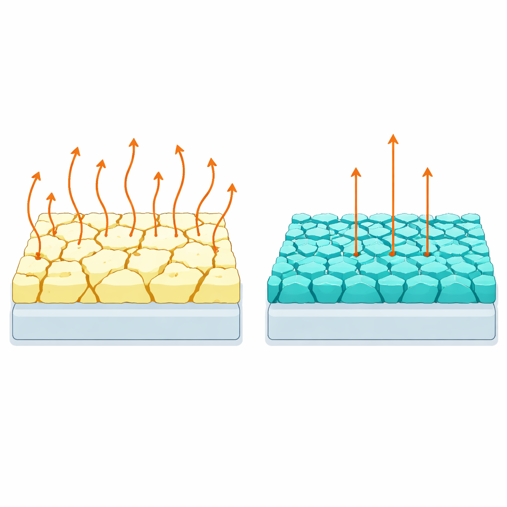
In many insulating films used on chips, the material is not a single perfect crystal but a patchwork of microscopic grains. Where these grains meet, so-called grain boundaries tend to disrupt the orderly arrangement of atoms. In conventional oxide insulators, such disruption creates extra electronic states inside the energy “gap” that should be empty. These hidden states act like stepping stones for charges, opening leakage paths that weaken the insulation and can ultimately limit the lifetime of memory cells or transistors.
A different kind of crystal with gentle joins
The material at the heart of this work, Sb2O3, belongs to a family called inorganic molecular crystals. Instead of atoms being locked together in a rigid network, they group into small cage-like molecules that touch each other only through weak van der Waals forces—soft attractions rather than strong chemical bonds. The authors show that thin films of Sb2O3 can be deposited by an industry-friendly thermal evaporation process while keeping these molecular cages intact. The result is a polycrystalline film only about 10 nanometers thick, containing countless grains separated by boundaries that resemble gentle molecular contacts instead of broken bonds.
Putting the film to the electrical test
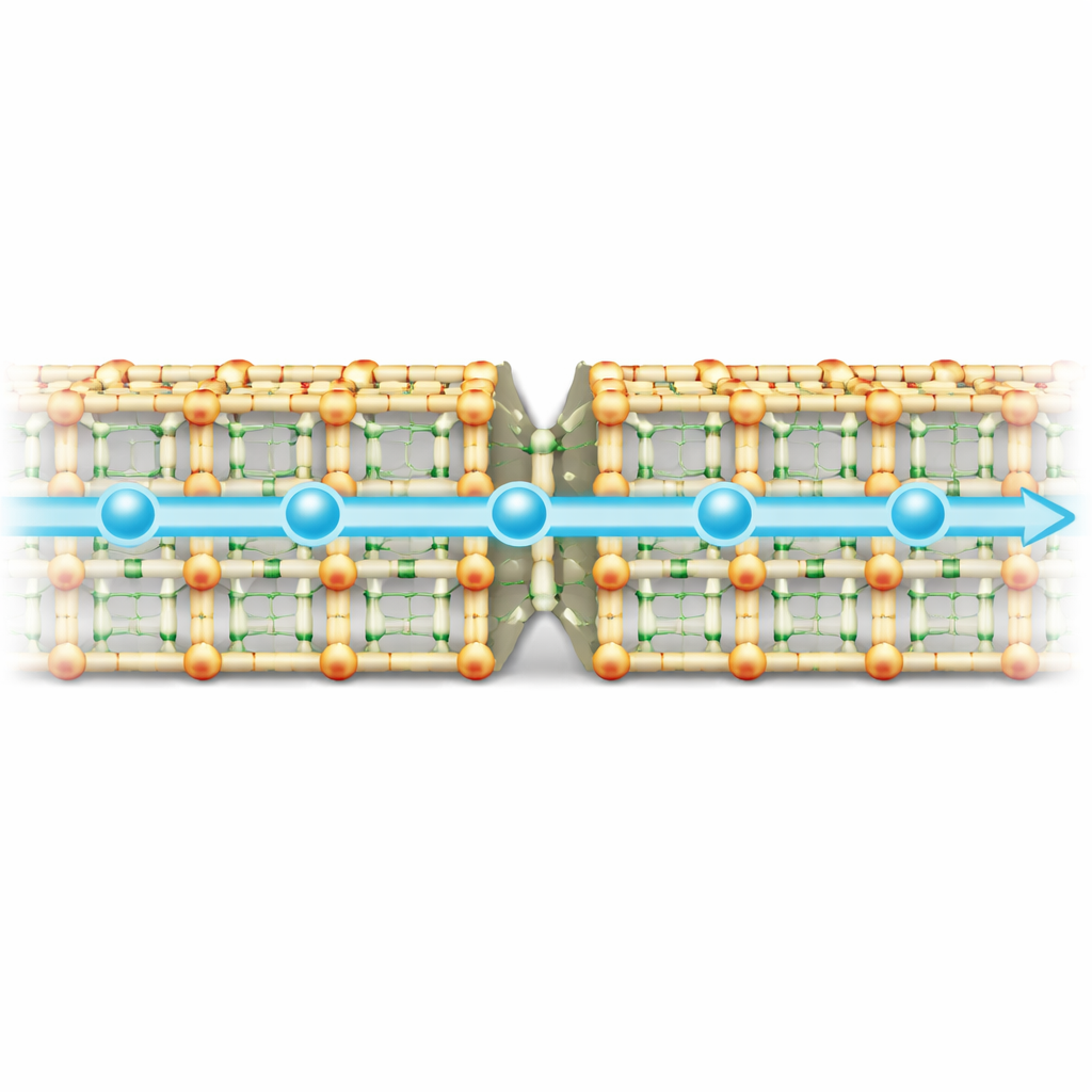
To see how well this film blocks current, the team sandwiched it between a silicon bottom electrode and a metal top electrode, making tiny capacitors with millions of grains in each device. Measurements over a wide range of temperatures revealed a remarkably low leakage current, far better than what would be expected if grain boundaries provided easy routes for charges. The way current increased with voltage matched a textbook tunneling process through a clean barrier, rather than mechanisms that rely on defect sites inside the insulator. This already hinted that the film contained very few electrically active flaws, even at its numerous grain boundaries.
Looking between grains from atoms to nanometers
The researchers combined high-resolution electron microscopy with powerful computer simulations to zoom in on what happens at and near the boundaries. Electron micrographs confirmed that the film is made of small grains about as thick as the film itself, meaning many boundaries run all the way from one electrode to the other. First-principles quantum calculations compared various realistic surface and boundary structures in Sb2O3 with a perfect bulk crystal. Unlike traditional oxides, these models showed that keeping whole molecular cages intact at the boundary prevents the formation of mid-gap states. Even explicit twin grain boundaries had band structures almost indistinguishable from the ideal crystal, indicating that the boundaries are electronically “quiet.”
Probing single grains with a sharp tip
To test this prediction directly, the team used conductive atomic force microscopy, which scans the surface with a nanoscale probe that can measure local currents. The surface topography revealed where the grain boundaries lie, thanks to slight grooves formed during growth. The researchers then recorded current–voltage curves at more than a hundred points, both within grains and exactly on boundaries. The average electrical response from the two regions overlapped almost perfectly and followed the same tunneling behavior. Current maps showed occasional tiny spots of higher conductivity, but these did not line up with the grain pattern and changed from scan to scan, suggesting random traps rather than systematic weak lines along the boundaries.
What this means for future electronics
The key message for non-specialists is that not all internal “cracks” in a crystal are harmful. In Sb2O3 molecular films, grain boundaries behave almost invisibly from an electrical point of view: they do not create extra leakage paths or significantly weaken the insulation. Because these films can be deposited with standard vacuum tools and are compatible with 2D semiconductors, they offer a promising route to reliable gate dielectrics in next-generation low-power devices. By showing that van der Waals grain boundaries can be electrically inert, this work may allow engineers to relax the demand for large single crystals and still build high-performance, scalable electronics.
Citation: Liu, K., Huang, B., Yuan, Y. et al. van der Waals grain boundaries with inert electrical behaviors in inorganic molecular dielectric film. Nat Commun 17, 2257 (2026). https://doi.org/10.1038/s41467-026-69066-z
Keywords: van der Waals dielectrics, grain boundaries, antimony trioxide, 2D electronics, gate insulators