Clear Sky Science · en
High quality-factor terahertz phonon-polaritons in layered lead iodide
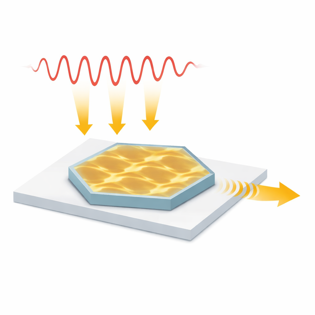
Light Waves Squeezed into Tiny Spaces
Smartphones, medical scanners, and security systems all rely on light, but not just the kind we see with our eyes. This study shows how a familiar chemical, lead iodide, can trap and guide a very long-wavelength form of light—terahertz radiation—into spaces hundreds of times smaller than its natural size. That ability could one day shrink bulky terahertz devices onto a chip, enabling sharper imaging, faster wireless links, and new ways to probe materials and molecules.
A New Way to Tame Terahertz Light
For years, researchers have learned to steer special light–vibration waves called phonon-polaritons in ultra-thin crystals such as hexagonal boron nitride. These waves occur when light couples strongly to the natural shaking of atoms in a solid, and they can travel in highly confined channels—much tighter than ordinary optics allow. Until now, most successes have been at mid-infrared frequencies. At longer terahertz wavelengths, where many useful signals lie, materials have been too lossy and the experiments too challenging. The authors show that layered lead iodide (PbI2) overcomes these obstacles, supporting long-lived, tightly confined waves deep in the terahertz range.
Why Lead Iodide Stands Out
Lead iodide is built from flat atomic sheets weakly stuck together, a so‑called van der Waals structure. This geometry makes the material behave very differently along and across the layers. In certain terahertz frequency bands, the way it responds to electric fields flips sign between directions, forcing light and lattice vibrations into unusual, strongly angled paths known as hyperbolic modes. Earlier optical studies hinted that PbI2 would have an exceptionally wide operating band and strong directional behavior, but its potential for nanoscale terahertz optics had not been explored. The team also notes a practical bonus: the atomic masses in lead iodide vary very little from sample to sample, which reduces disorder and helps the vibrations live longer, a key ingredient for high-quality polaritons.
Imaging Waves Smaller Than the Wavelength
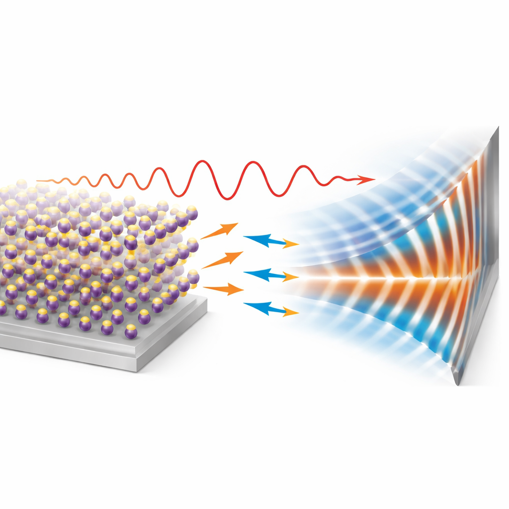
To actually see these hidden waves, the researchers turned to scattering-type scanning near-field optical microscopy, a technique that uses a sharp metallic tip like a tiny antenna. They illuminated thin PbI2 flakes with terahertz light and scanned the tip across the surface, recording the faint scattered signal. The images revealed rippling patterns inside the crystals, with the spacing between ripples changing in a predictable way as the crystal thickness varied. Careful analysis and comparison with theory showed that these patterns were hyperbolic phonon-polaritons whose wavelengths were compressed by factors up to 264 in a 144‑nanometer film—and likely more than 300 in slightly thinner samples.
Measuring How Well the Waves Travel
Beyond static images, the group used a time-resolved version of the same microscope to watch how the waves behaved across a broad range of terahertz frequencies. By recording spectra at many points across a crystal edge, they observed how the bright fringes shifted and stretched as frequency changed, matching the expected dispersion of the polaritons. From these measurements they extracted a figure-of-merit that captures how far the waves travel before fading. Values reached about 17, comparable to or better than many celebrated materials in the infrared. They also showed that crystal edges can naturally launch these waves and that PbI2 flakes act as effective miniature resonators on both insulating and metallic supports, forming clear standing-wave patterns.
From Curious Crystal to Future Devices
Putting these pieces together, the work identifies layered lead iodide as a powerful platform for terahertz nanophotonics. It combines strong directionality, low loss, and extreme confinement in a material that is relatively easy to grow and already known in X‑ray detectors and solar-cell research. Because it is a semiconductor and can be stacked with other two-dimensional layers, PbI2 could host active components—such as switches, detectors, and compact waveguides—that harness polariton waves instead of conventional light. In simple terms, this crystal lets engineers draw very fine "light wires" for terahertz radiation, opening a path toward smaller and more capable devices that operate in a spectral range still largely untapped by everyday technology.
Citation: Santos, C.N., Feres, F.H., Hannotte, T. et al. High quality-factor terahertz phonon-polaritons in layered lead iodide. Nat Commun 17, 2356 (2026). https://doi.org/10.1038/s41467-026-69027-6
Keywords: terahertz nanophotonics, phonon polaritons, lead iodide, two-dimensional materials, near-field microscopy