Clear Sky Science · en
Growth of rhombohedral-stacked single-crystal WS2/MoS2 vertical heterostructures
Building Better Electronic Sandwiches
Many of the most exciting ideas in future electronics—ultra-thin phones, flexible solar cells, and tiny quantum devices—depend on stacking sheets of materials only a few atoms thick, like making a sandwich at the scale of molecules. This paper shows how to reliably grow such “atomic sandwiches” made of two popular semiconductor layers, WS2 and MoS2, over areas big enough for real-world devices, while also giving them a built-in electric polarization that could power new memory and sensing technologies.
Why Stacking Atom-Thin Sheets Is So Hard
Researchers love vertical stacks of two-dimensional materials because they can mix and match different layers to create properties that do not exist in nature, such as unusual light emission or switchable electric polarization. Until now, the standard way to build these stacks has been painfully slow and messy: peel off tiny flakes with sticky tape and manually place them on top of each other. This approach works for lab experiments but leaves behind trapped dirt, gives inconsistent results, and produces areas only micrometers across—far too small for mass-produced chips. Growing the stacks directly in a furnace using chemical vapour deposition promises clean and large films, but there has been a stubborn roadblock: the upper layer can choose between two mirror-image orientations that are almost equally favourable, leading to a patchwork of domains instead of a single, well-aligned crystal.
Turning Defects from a Bug into a Feature
Chen and colleagues tackled this problem by focusing on tiny imperfections—missing sulphur atoms—in the bottom MoS2 layer. Using quantum-mechanical simulations, they showed that these sulphur vacancies are much easier to form at the edges of atomic “steps” on the MoS2 surface than on the flat regions. These vacancies expose reactive metal atoms that act like docking sites for the incoming WS2 layer. Crucially, this docking only strongly favours one of the two possible stacking orientations. As a result, once a WS2 island begins to grow at such a vacancy-decorated step, it is overwhelmingly likely to adopt the same orientation everywhere, breaking the previous symmetry that caused disorder. 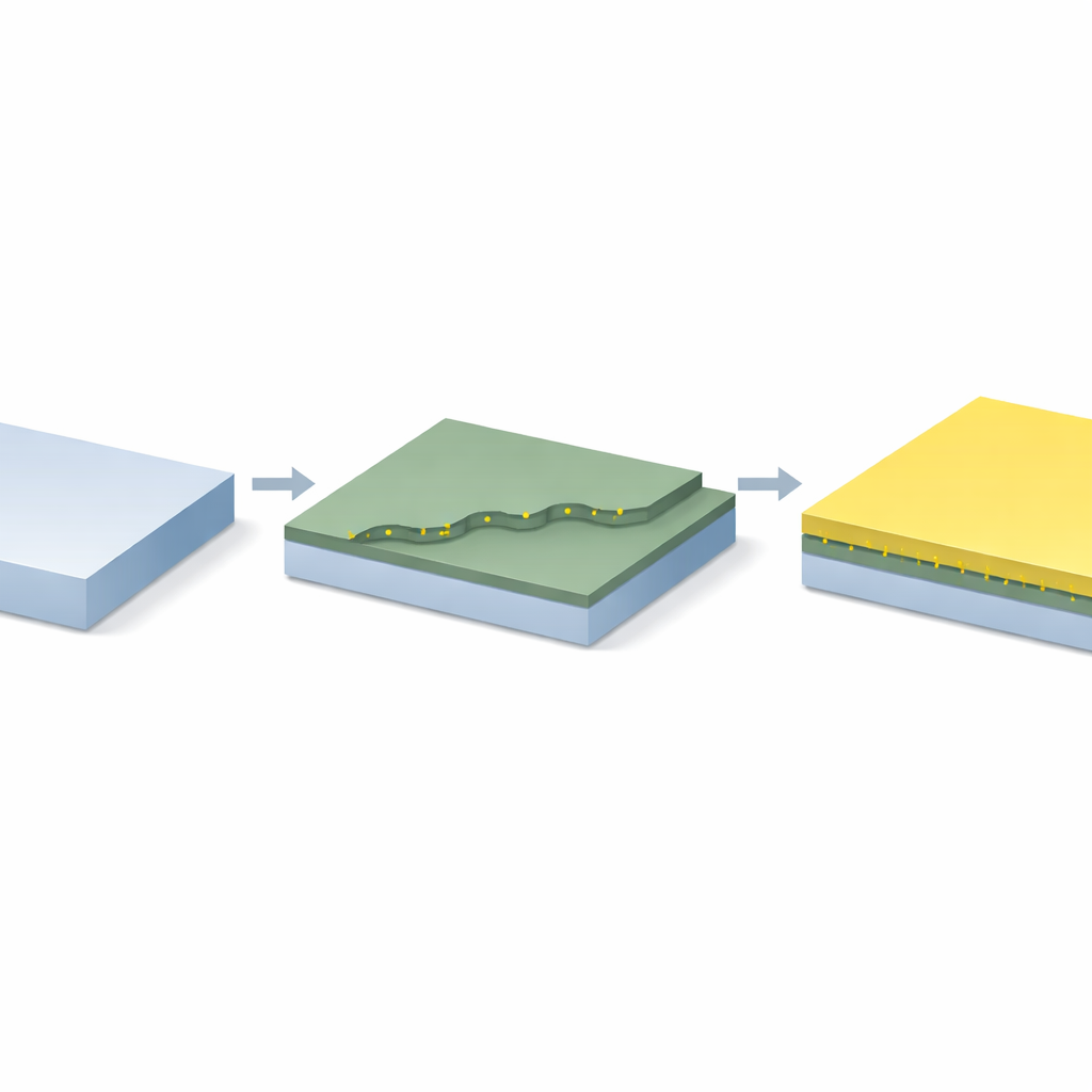
Guided Growth to Centimeter-Scale Single Crystals
Guided by this insight, the team developed a multi-step growth recipe. First, they grew large, single-crystal MoS2 sheets on sapphire by carefully stitching together aligned triangular islands. Next, they gently heated these MoS2 films in vacuum to encourage sulphur atoms near step edges to leave, creating a controlled population of vacancies. Finally, they introduced a tungsten source to grow WS2 on top. At short growth times, they observed that WS2 islands formed primarily along the step edges and all pointed in the same direction. With longer growth, these islands merged seamlessly into a continuous WS2 film perfectly aligned with the MoS2 beneath it, yielding a 1 cm × 1 cm single crystal of rhombohedrally stacked WS2/MoS2—gigantic by the standards of atom-thick materials. They further showed that the same vacancy-guided strategy also works when replacing MoS2 with another related material, WSe2, suggesting a broadly applicable method. 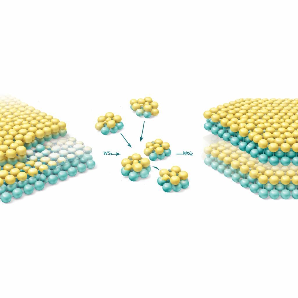
Proving the Crystal Quality and Hidden Electric Order
To confirm that their films were truly single crystals with the desired stacking pattern, the researchers deployed a battery of imaging and optical tools. Light-based measurements of colour emission and atomic vibrations showed uniform signals from both WS2 and MoS2 across millimetre and centimetre scales, indicating even composition. Atomically resolved force microscopy revealed that neighbouring WS2 islands joined without forming grain boundaries, while advanced electron microscopy provided direct pictures of the rhombohedral stacking at the atomic level. Using a nonlinear optical technique sensitive to symmetry, they mapped the entire film and found the same stacking everywhere. Most intriguingly, electrical and mechanical probes revealed ferroelectric behaviour—an internal electric polarization that can be switched by an external voltage—arising from the specific way the two layers are offset. Devices made from these stacks displayed higher charge mobility and a built-in photoelectric response, meaning they can generate current from light without an external power supply.
What This Means for Future Devices
In essence, this work turns unavoidable defects into precise tools for steering crystal growth. By using sulphur vacancies at step edges to dictate where and how the upper WS2 layer forms, the authors demonstrate a robust recipe for making large, single-crystal, rhombohedral WS2/MoS2 films that combine excellent electronic quality with switchable electric polarization and self-powered light detection. For a lay reader, the takeaway is that we are learning to “program” matter at the atomic level during growth, opening a path toward practical, wafer-scale production of ultra-thin, energy-efficient electronics and novel memory and sensor technologies built from stacks only a few atoms thick.
Citation: Chen, J., Guo, Y., Zhang, Y. et al. Growth of rhombohedral-stacked single-crystal WS2/MoS2 vertical heterostructures. Nat Commun 17, 2172 (2026). https://doi.org/10.1038/s41467-026-68935-x
Keywords: 2D materials, van der Waals heterostructures, single-crystal growth, ferroelectric devices, chemical vapor deposition