Clear Sky Science · en
Localized 2D/3D heterojunction enhances photovoltage for perovskite-organic tandem solar cells
Why this solar study matters
Solar panels are getting cheaper and more common, but today’s single-layer designs are bumping up against efficiency limits. This research shows a clever way to stack different light-absorbing materials and fine‑tune the tiny boundary between them, squeezing more voltage and stability out of next‑generation “tandem” solar cells. The advance could help future panels turn more sunlight into electricity without a big jump in cost.
Stacking layers for more sunlight
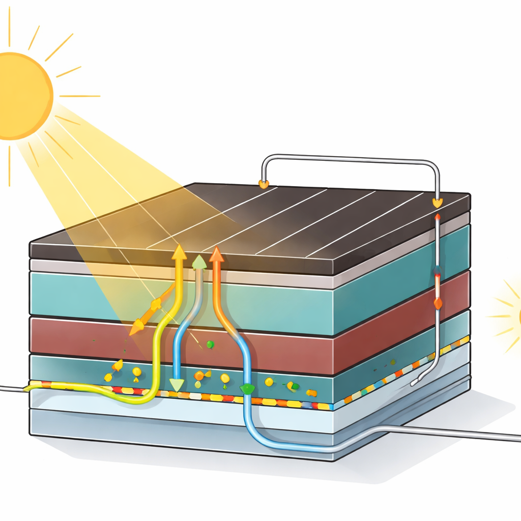
Standard solar cells use one active layer to capture light, which caps how much power they can deliver. Tandem solar cells take a different approach: they stack two or more layers, each tuned to a different color range of sunlight. In this work, the team uses a wide-bandgap perovskite layer on the front to catch higher‑energy light, and a narrow‑bandgap organic layer beneath it to harvest red and near‑infrared light. In principle, this design should deliver higher voltages and efficiencies. In practice, however, the upper perovskite layer usually falls short because of hidden energy losses at its buried interface—the internal contact that you never see but that strongly controls how charges leave the material.
Fixing a hidden weak spot
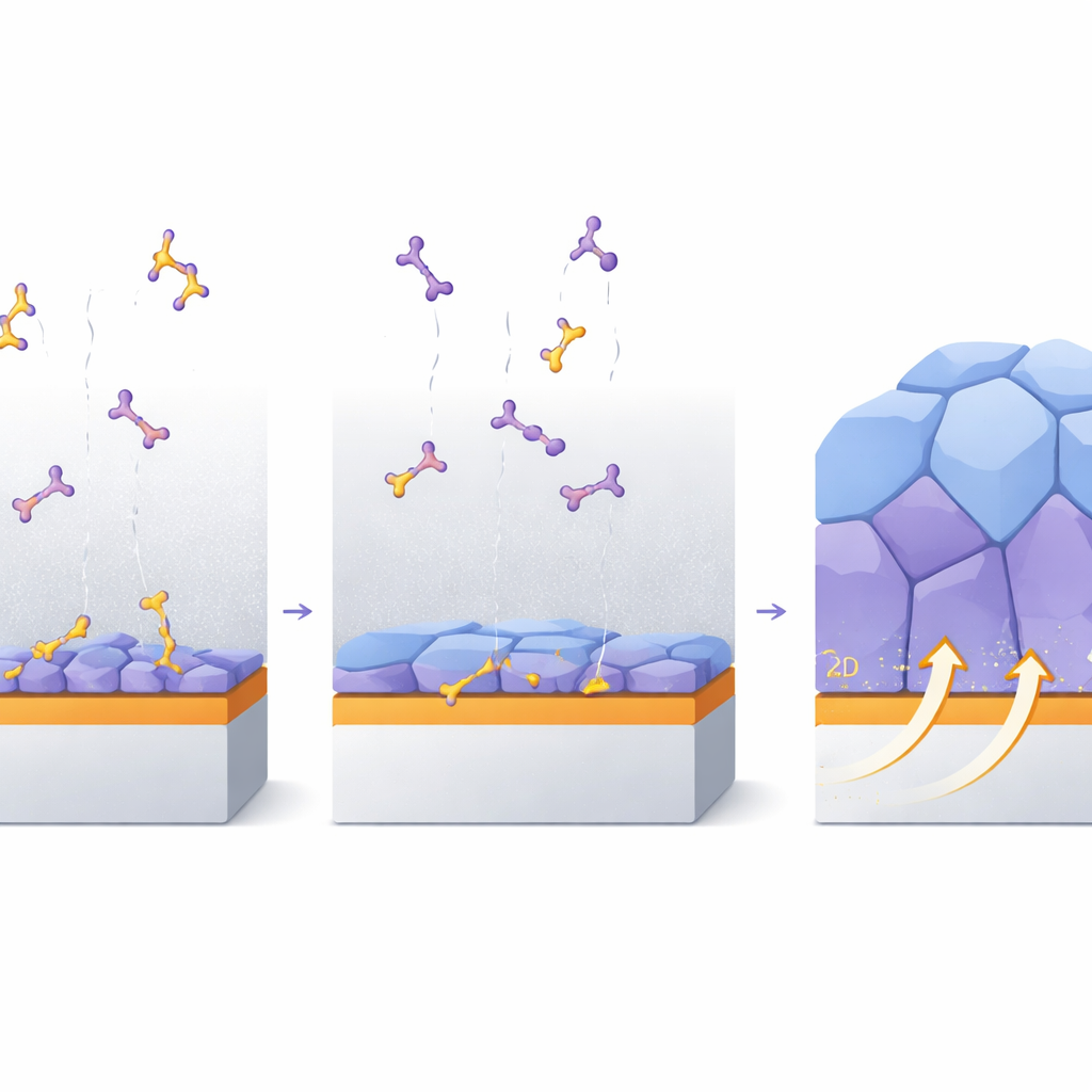
The buried interface between the transparent electrode and the perovskite is often riddled with defects and poor energy alignment. These flaws act like tiny traps where excited charges recombine before doing useful work, limiting the photovoltage. The authors tackle this weak spot by designing a special self‑assembled monolayer (SAM) molecule called CbzBT‑B. It forms an ultrathin, orderly layer on the transparent contact and is engineered to have both the right energy level and a sulfur‑containing head group that can strongly attract positively charged ammonium ligands used in perovskite processing. This targeted interaction localizes these ligands exactly where they are needed instead of letting them drift randomly into the bulk material.
Building a smart boundary inside the cell
When the perovskite layer grows on top of this tailored SAM, the anchored ligands help form a very thin two‑dimensional (2D) perovskite region right at the buried interface, while the rest of the film remains a high‑quality three‑dimensional (3D) perovskite. This creates a localized 2D/3D “heterojunction”—a smart boundary that guides how charges move. Using a suite of advanced imaging and spectroscopy tools, the researchers show that these 2D regions stay confined near the interface and along grain boundaries, rather than spreading throughout the crystal where they would hinder charge transport. The engineered boundary also steers how the perovskite crystals nucleate and grow, yielding smoother films with preferred crystal orientation and fewer structural voids.
Cleaner charge flow and higher voltage
Because the boundary is better organized and less defective, charges can now escape more easily instead of getting trapped. Time‑resolved optical measurements reveal slower recombination and more efficient hole extraction at this interface. Electrical profiling techniques show that defect densities at the buried side drop by roughly an order of magnitude, while charge mobility improves and energy levels line up more favorably for charge transfer. As a result, the wide‑bandgap perovskite cells reach photovoltages of 1.30, 1.38, and 1.42 volts for bandgaps of 1.68, 1.79, and 1.85 electron volts, respectively—each exceeding 90 percent of the theoretical maximum for that material, a key benchmark in solar research.
Turning better cells into better tandems
Armed with this improved wide‑bandgap perovskite subcell, the team then stacks it with a carefully tuned organic rear cell to create a monolithic perovskite‑organic tandem. Thanks to the high voltage and low loss of the front cell and a well‑designed connecting layer between the two, the tandem reaches a power conversion efficiency of 27.11 percent, with an independently certified value of 26.3 percent—among the highest reported for this class of devices. The cells also hold up under continuous operation and thermal cycling, keeping most of their initial performance over hundreds of hours, which points to better durability than many earlier perovskite designs.
What this means for future solar panels
In simple terms, the study shows that paying careful attention to an invisible internal boundary can unlock both higher voltage and longer life in advanced solar cells. By using a purpose‑built molecular layer to pin down a thin 2D perovskite at exactly the right place, the researchers turn a problematic interface into a helpful one that cleans up defects and speeds charge extraction. If this approach can be scaled and integrated into manufacturing, it could help push tandem solar panels closer to their full potential, delivering more clean electricity from the same patch of sunlight.
Citation: Chen, M., Jiang, W., Wang, D. et al. Localized 2D/3D heterojunction enhances photovoltage for perovskite-organic tandem solar cells. Nat Commun 17, 2093 (2026). https://doi.org/10.1038/s41467-026-68904-4
Keywords: perovskite solar cells, tandem photovoltaics, interface engineering, 2D 3D heterojunctions, photovoltage enhancement