Clear Sky Science · en
Imaging multilevel exciton transport enabled by correlated electronic states
Why tiny light-carrying particles matter
Modern technologies from ultrafast computers to energy‑efficient data links increasingly rely on excitons—fleeting pairings of electrons and holes that carry energy instead of electrical current. If engineers could steer these excitons with the same precision as electrons in a transistor, they could build logic circuits and optical interconnects that are faster and use far less power. This study shows how to finely tune exciton motion in atomically thin materials by taking advantage of exotic electronic states that form in carefully stacked layers only a few atoms thick.
Building a tiny layered playground for excitons
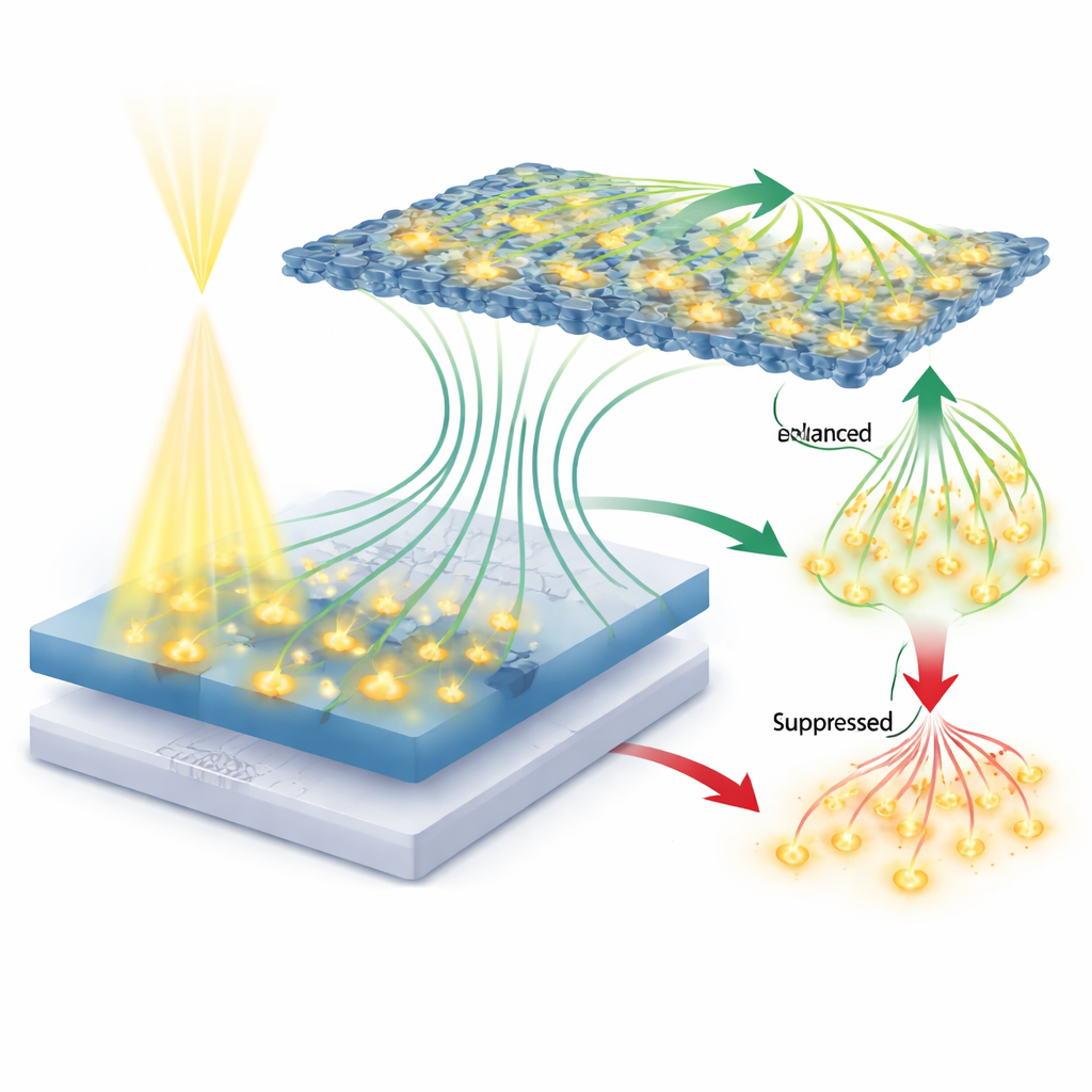
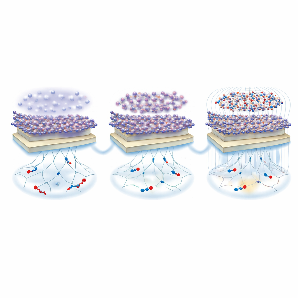
The researchers constructed a nanoscale device made of two different atomically thin semiconductors, WS2 and WSe2, separated by an ultrathin insulating spacer of hexagonal boron nitride. The bottom WSe2 layer acts as an exciton “sensor,” where light creates and tracks the motion of excitons. Above it sits a twisted pair of WS2 sheets that form a moiré superlattice—a repeating interference pattern on the scale of billionths of a meter. By applying a voltage gate, the team can add or remove electrons in this moiré layer, driving it between metallic states where electrons are mobile and insulating states where they arrange themselves into ordered patterns called generalized Wigner crystals.
Filming excitons in space and time
To see how these changes in the upper layer affect excitons in the sensor below, the team used an ultrafast optical microscope that combines a tightly focused pump pulse with a delayed probe pulse. The pump pulse injects excitons into a small spot in the WSe2 layer, while the probe scans across the region and records how the reflected signal changes over time. This setup achieves a remarkable 200‑femtosecond time resolution and 50‑nanometer spatial resolution, allowing the researchers to watch excitons spread out like a tiny expanding cloud. By fitting these evolving profiles with a simple diffusion model, they extracted how quickly excitons move and how long they survive before recombining.
How ordered electrons choke or boost exciton flow
The key control knob is the electronic state of the twisted WS2 bilayer. When this moiré system behaves like a metal, its high ability to screen electric fields smooths out microscopic charge irregularities in the environment. As a result, excitons in the nearby WSe2 layer experience fewer obstacles and diffuse more freely. But at special “fractional filling” conditions—specific electron densities set by the gate voltage—strong interactions force electrons in the moiré lattice into Wigner crystal patterns, forming stripes or triangular arrays. These insulating states have a much lower dielectric response, meaning they screen electric fields poorly. That increases the disorder seen by excitons, sharply reducing how far and how fast they can travel.
Shorter lives, shorter journeys
The ordered insulating phases do more than just slow excitons down; they also make them shorter‑lived. When the dielectric constant of the WS2 layer drops, excitons in WSe2 feel a stronger attraction between their electron and hole components. This pulls the pair closer together, increasing their binding energy and overlap, which in turn accelerates their recombination. Measurements show that at fractional fillings where Wigner crystals form, both the diffusion coefficient and the exciton lifetime fall in tandem, leading to a drastic shrinkage of the distance excitons can cover. As temperature rises, thermal motion gradually melts these ordered electronic patterns, and the suppression of exciton transport fades away, revealing a characteristic temperature for each correlated state.
From quantum patterns to future light-based circuits
Taken together, these results demonstrate a way to use correlated electronic states—ordered arrangements of electrons dictated by quantum interactions—to dynamically regulate exciton transport in a nearby layer. Instead of relying on static device parameters such as fixed strain or permanent interfaces, this approach allows multilevel control of exciton flow simply by tuning voltage and temperature. The ultrafast optical method developed here acts as a sensitive, contact‑free probe of complex quantum phases while directly revealing how they reshape the motion and lifetime of excitons. Such control could underpin future excitonic logic elements, low‑power photonic links, and programmable quantum materials where electronic and light‑carrying quasiparticles are engineered to work together.
Citation: Liu, H., Chen, S., Xu, H. et al. Imaging multilevel exciton transport enabled by correlated electronic states. Nat Commun 17, 2137 (2026). https://doi.org/10.1038/s41467-026-68868-5
Keywords: exciton transport, moiré materials, Wigner crystal, two-dimensional semiconductors, ultrafast microscopy