Clear Sky Science · en
Polarization-modulated programmable photovoltaic performance of a designed ferroelectric heterojunction
Smart solar sensors for future vision
Imagine a camera chip that not only captures light, like today’s image sensors, but also thinks about what it sees—picking out edges, shapes, and patterns on its own while using very little power. This paper reports a new kind of light‑sensing device that does exactly that, by combining an unusual solar effect with a carefully designed layered material. The result is a “programmable solar pixel” whose response to light can be written, erased, and reversed, opening doors to smarter, more efficient machine vision.
Why regular solar cells hit a wall
Conventional solar cells and many light sensors rely on p–n or Schottky junctions, where the useful voltage is fundamentally tied to the material’s band gap. This link underlies the well‑known Shockley–Queisser limit and makes it hard to go beyond certain efficiency and voltage thresholds. It also restricts how flexibly one can tune the device response after fabrication. As neuromorphic, or brain‑inspired, vision systems emerge—requiring ultrafast, sensitive, and reconfigurable pixels that can process information in place—these limits become a bottleneck. Engineers need devices whose behavior under light can be dynamically programmed rather than fixed at the factory.

Using a special crystal to break the rules
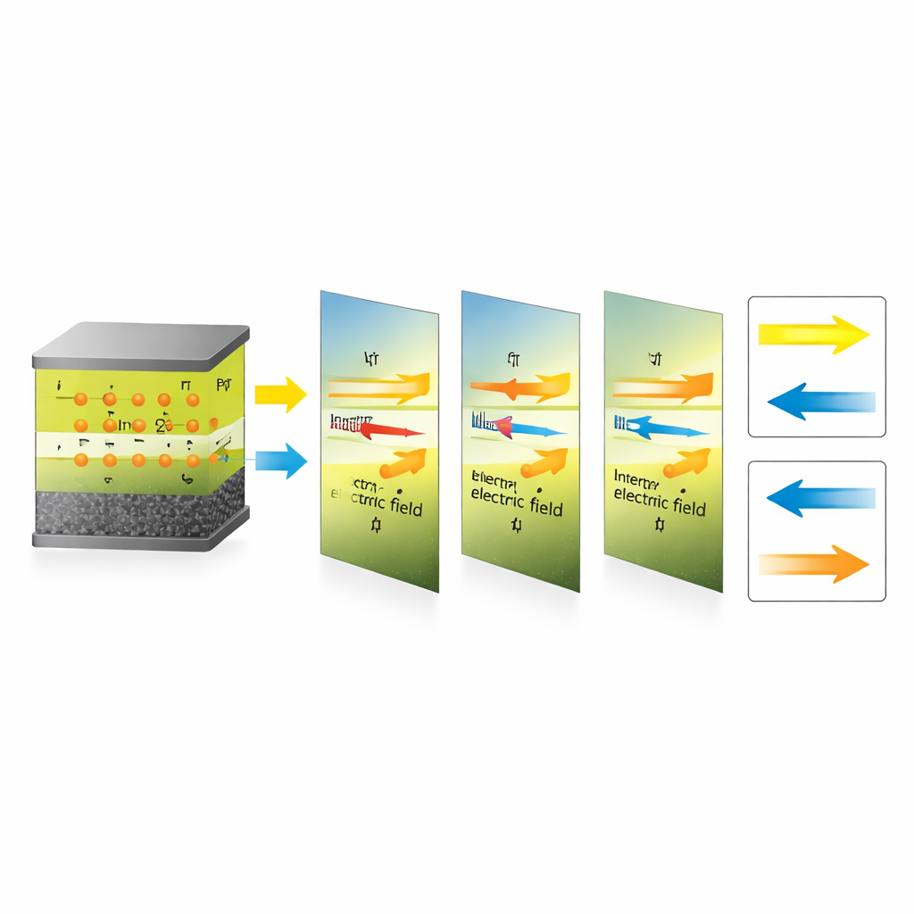
The authors turn to a layered ferroelectric crystal called CuInP₂S₆ (often shortened to CIPS), which shows a bulk photovoltaic effect. In such materials, internal electric polarization separates photo‑generated charges without the usual built‑in junction field, allowing voltages that can exceed the band‑gap‑based ceiling of ordinary semiconductors. CIPS has two key advantages: its polarization can be flipped at room temperature, and copper ions inside the layers can move in response to an electric field, reinforcing or even reversing the local polarization. By stacking CIPS between a platinum bottom contact and a graphene top contact, the researchers build an asymmetric sandwich whose internal barriers and light response can be steered by electric pulses.
Writing and flipping the light response
Experiments on this Pt/CIPS/graphene heterojunction show that a modest laser produces a strong photocurrent that can be increased by about a factor of ten simply by changing the prior voltage pulse applied to the device. Remarkably, the direction of the photocurrent can be switched from positive to negative and back again in a controlled way. Detailed measurements as the team varies temperature and bias history reveal that this behavior depends on the ferroelectric state of CIPS rather than on simpler effects such as heating or interface charging. Computer simulations based on quantum‑mechanical calculations back up this picture: when copper ions shift within and between the crystal layers, they alter the energy landscape at the contacts, reshaping how electrons and holes move from CIPS into graphene and platinum under illumination.
Ion motion as a hidden control knob
By tracking current–voltage curves while gradually increasing positive or negative programming pulses, the researchers map out a rich, repeatable pattern of switching. Under some conditions, copper ions move mainly within a given layer, partially canceling the initial polarization; under stronger fields, they hop between layers, rebuilding a polarization that can even oppose the applied field. Each configuration sets a different internal barrier profile and therefore a different light response, yet these states persist without power—meaning the device remembers how it was programmed. Comparisons with a symmetric graphene/CIPS/graphene version confirm that the asymmetric contacts are essential for the unusual one‑sided switching seen here.
Turning pixels into tiny processors
Because each device’s light sensitivity can be smoothly tuned and even given a sign, it can act like a weighted connection in a neural network, implemented directly in hardware. The team demonstrates this by mapping image pixels onto arrays of such devices and using their photocurrents to perform the core multiply‑and‑add operations of common vision algorithms. In simulations based on measured device behavior, the system performs edge detection on a simple flower‑shaped image with a perfect F‑score of about 1, and carries out a small pattern‑classification task—distinguishing noisy versions of “X” and “T” patterns—with 100% accuracy, all within the sensor itself rather than on a separate processor.
What this means for future vision chips
In everyday terms, the authors have built a light‑powered element whose sensitivity and even sign can be dialed in like a memory bit, then used to both sense and pre‑analyze visual information. By harnessing the interplay between ferroelectric polarization and mobile copper ions in a layered crystal, they show how to break free from traditional solar cell limits and create reprogrammable, non‑volatile pixels. Such devices could underpin future cameras and sensors that do much of their thinking on the chip itself, enabling faster, more energy‑efficient artificial vision in everything from mobile gadgets to autonomous robots.
Citation: Men, M., Deng, Z., Zhao, Z. et al. Polarization-modulated programmable photovoltaic performance of a designed ferroelectric heterojunction. Nat Commun 17, 2096 (2026). https://doi.org/10.1038/s41467-026-68853-y
Keywords: ferroelectric photovoltaic, neuromorphic vision, van der Waals heterojunction, in-sensor computing, CuInP2S6