Clear Sky Science · en
Boosting carbon nanotube transistors through γ-ray irradiation
Cleaning Up the Future of Tiny Electronics
Modern life depends on ever-smaller, ever-faster computer chips, but conventional silicon technology is running into hard limits. This study explores an unusual helper from nuclear physics—high‑energy gamma rays—as a way to clean and boost next‑generation transistors built from carbon nanotubes. By gently zapping finished devices, the authors show they can cut wasteful leakage currents, improve switching behavior, and make electronics that shrug off radiation levels far beyond what silicon can survive.
Why Carbon Nanotubes Need a Makeover
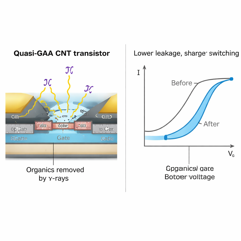
Carbon nanotube transistors are widely viewed as a leading candidate to pick up where shrinking silicon transistors leave off. They can switch faster, use less power, and are already being made in ways that fit into commercial chip factories. But there is a hidden problem: organic molecules left over from nanotube sorting and device fabrication cling to the interface between the nanotubes and the insulating layers that control them. These molecular leftovers create unwanted electronic “stepping‑stones” inside the nanotube’s energy gap, allowing charges to sneak through when the device is supposed to be off and making the switch from off to on less sharp. Existing cleanup methods—chemical treatments, high‑temperature baking, or focused electron beams—either do not work well enough, risk damaging the nanotubes, or are too slow and expensive for industrial use.
Turning Gamma Rays into a Precision Cleaning Tool
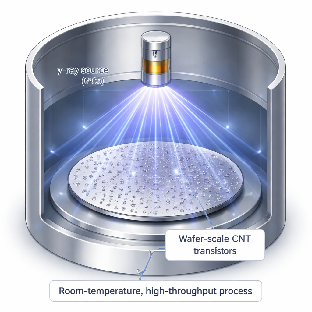
The researchers propose a counterintuitive solution: use intense gamma rays, emitted by a cobalt‑60 source, to selectively break apart the weak chemical bonds in the surrounding organic molecules while leaving the robust carbon nanotubes essentially unharmed. Gamma rays carry far more energy than the electrons used in microscopes or the gentle heat of annealing ovens, and they can penetrate entire wafers at once. Careful measurements showed that pristine nanotubes maintained their ordered structure even after an enormous total dose of 100 megarad, while characteristic signals from the polymers used to sort the nanotubes shrank dramatically. Spectroscopy revealed that bonds associated with disordered, low‑energy configurations were converted into stronger, more graphitic bonds, consistent with organic contaminants being broken down and reorganized rather than the nanotube lattice itself being damaged.
Building and Zapping Advanced Transistor Designs
To connect this microscopic chemistry to real devices, the team fabricated so‑called quasi gate‑all‑around carbon nanotube transistors on full four‑inch wafers using standard chip‑making steps. In this layout, a very thin network of nanotubes is sandwiched between top and bottom gate electrodes, giving better electrical control than a single gate while remaining easier to manufacture than the most advanced three‑dimensional silicon designs. Even before irradiation, these N‑type devices already showed strong on‑state currents at modest voltages and competitive switching sharpness. The authors then exposed many such transistors to increasing gamma‑ray doses without applying any electrical bias, periodically measuring how their behavior changed. Although a modest dose caused a temporary worsening—slightly higher leakage and softer switching—pushing the dose to 100 megarad reversed the trend, yielding higher on‑state current, about an order‑of‑magnitude lower off‑state leakage, and significantly improved subthreshold swing, a key measure of how decisively the device turns on and off.
Stable Performance at Factory Scale and in Harsh Environments
Importantly for real‑world use, these benefits were not limited to a handful of lucky devices. Across one hundred transistors on silicon wafers, and additional sets built on polymer‑based flexible substrates and with different channel layouts, gamma‑ray treatment consistently tightened device‑to‑device variation while cutting leakage and sharpening switching. The threshold voltage—the point where the device turns on—barely shifted, staying within about ten percent of the supply voltage even at the highest tested dose. This is striking when compared with conventional silicon transistors, which typically fail around one megarad even when specially hardened. The quasi gate‑all‑around nanotube design, combined with the inherent radiation hardness of carbon nanotubes, withstood a hundred times more total ionizing radiation without losing control. Because the gamma‑ray source can bathe many wafers at once at room temperature, the authors estimate that a single installation could process thousands of 12‑inch wafers per month, meeting industrial demands for throughput and cost.
What This Means for Everyday Technology
For non‑specialists, the key message is that the authors have turned a powerful, potentially destructive form of radiation into a finely tuned cleaning tool for future computer chips. By blasting away troublesome molecular clutter around carbon nanotubes, they lower unwanted “leaks” when transistors are off and make the on‑off switch sharper—both crucial for low‑power, reliable electronics. At the same time, the devices prove exceptionally resistant to radiation damage, making them attractive for spacecraft, nuclear facilities, and medical imaging systems where ordinary chips quickly degrade. In short, gamma‑ray processing offers a practical, factory‑friendly step that pushes carbon nanotube transistors closer to everyday use, from faster phones and data centers to electronics that can function where today’s silicon simply cannot.
Citation: Zhang, K., Gao, N., Zhang, J. et al. Boosting carbon nanotube transistors through γ-ray irradiation. Nat Commun 17, 1896 (2026). https://doi.org/10.1038/s41467-026-68673-0
Keywords: carbon nanotube transistors, gamma-ray processing, radiation-hardened electronics, low-power chips, post-Moore semiconductor technology