Clear Sky Science · en
Inverse-designed nanophotonic neural network accelerators for ultra-compact optical computing
Why shrinking computers made of light matters
Modern artificial intelligence runs on vast electronic hardware that consumes enormous energy and generates heat. This study explores a very different path: using tiny patterns of light on a chip, rather than streams of electrons, to carry out parts of neural network computation. The authors show that by “sculpting” light at the nanoscale, they can build ultra‑compact optical accelerators that recognize handwritten digits and medical images while using far less space and, in principle, far less energy than today’s electronics.
Tiny chips that think with light
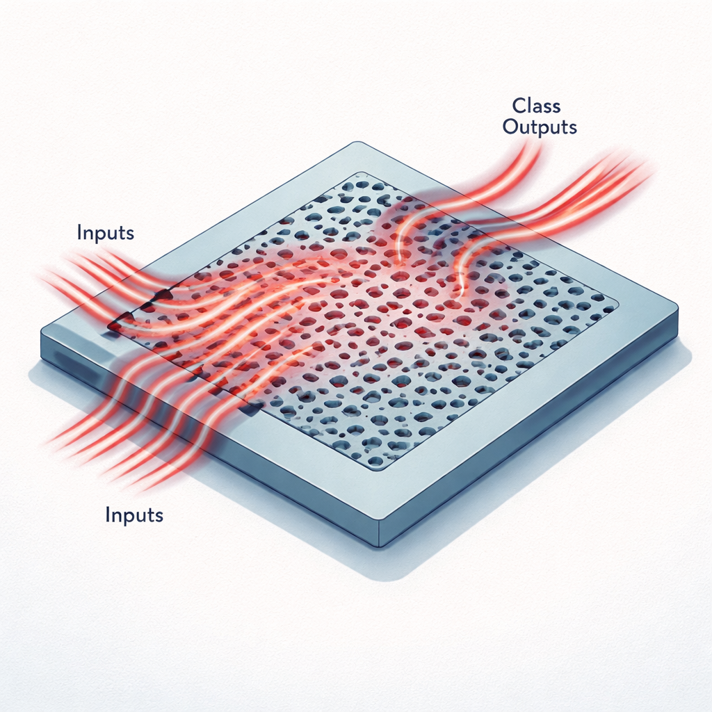
Instead of wires and transistors, these accelerators use a flat piece of silicon patterned with holes and channels smaller than the wavelength of infrared light. Data from an image are first compressed into a small set of numbers, which are then encoded as the brightness of light entering several narrow waveguides at a single telecom wavelength. As this light flows into the patterned region, it is scattered, interferes with itself, and is redirected toward a handful of output waveguides. Each output corresponds to a possible class, such as one of ten digits in the MNIST dataset or one of six categories in a medical imaging set called MedNIST. The pattern of optical power at the outputs plays the same role as the last layer of a digital neural network.
Letting algorithms draw the optical blueprint
Designing such a structure by hand would be nearly impossible, because every tiny “voxel” of material can change how light moves. The researchers instead use an inverse‑design approach: they start from a random pattern of silicon and glass, simulate how light propagates through it in three dimensions, and then adjust the pattern to reduce a loss function that measures classification errors. They take advantage of the linearity of Maxwell’s equations—the laws that govern light—to make this training efficient. Rather than simulate every training image separately, they simulate each input channel once, then reconstruct the fields for all images as linear combinations of these precomputed fields. A mathematical technique called the adjoint method then provides exact gradients that tell the algorithm how to nudge every voxel to improve performance.
Compact image classifiers on a grain of sand
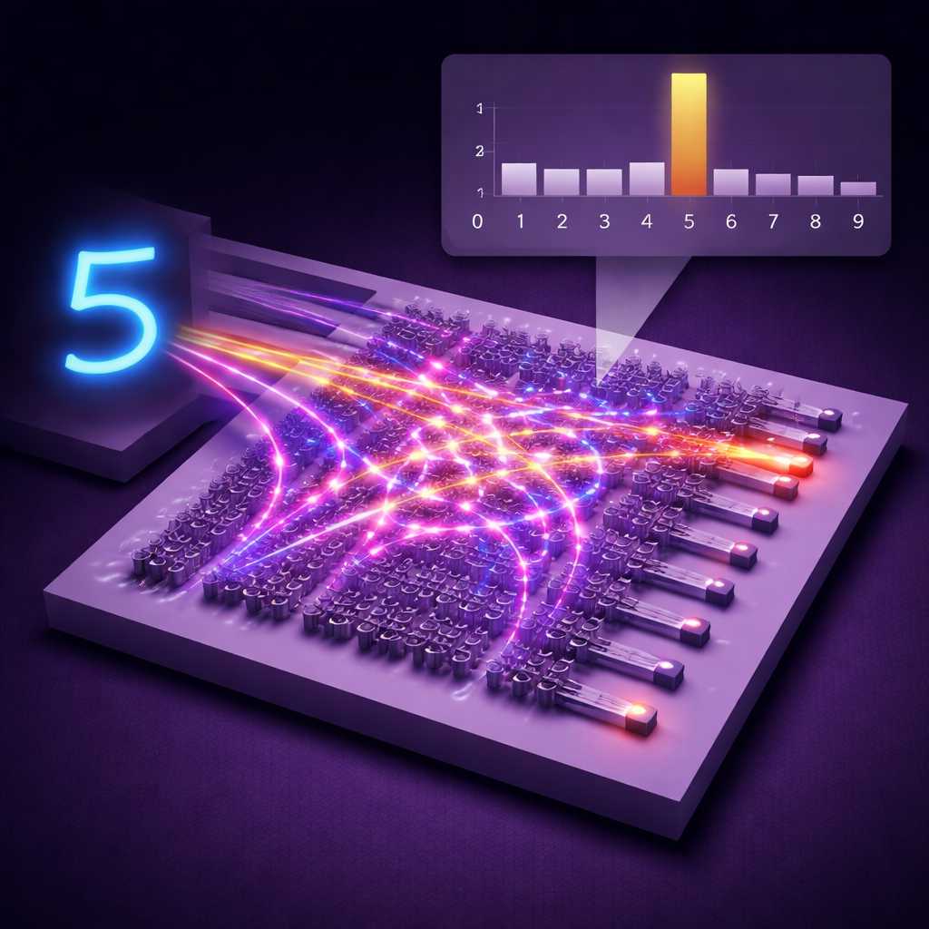
Using this strategy, the team designed two nanophotonic neural network accelerators on a standard silicon‑on‑insulator platform. One, just 20 by 20 micrometers in area, classifies handwritten digits from the MNIST dataset; the other, 30 by 20 micrometers, classifies medical images from MedNIST. In simulations, these tiny devices achieved accuracies of 97.8% and 99.1%, respectively. Fabricated versions of the same designs, tested with real lasers and detectors, reached 89% accuracy for MNIST and 90% for MedNIST—remarkable numbers given the chips’ minute size. The optical structures pack roughly 160,000 to 240,000 trainable parameters into areas smaller than a grain of dust, corresponding to about 400 million parameters per square millimeter.
Built for speed, efficiency, and scale
Because the devices are passive—there are no moving parts or reprogrammable elements during inference—they do not need continuous tuning once fabricated. The “weights” of the neural network are hard‑wired into the geometry of the nanostructure, so calculation happens at the speed of light with essentially in‑memory processing: light enters with encoded data and exits already mixed into class scores. The training method is also designed to be scalable. Each optimization step requires only a fixed number of full‑physics simulations determined by the number of inputs and outputs, not by the size of the dataset, and these simulations can be distributed across multiple graphics processing units. The authors further outline how multiple such optical cores could be stacked with photodetectors between them, much like layers in a deep neural network, and how multiplexing in wavelength or time could increase throughput.
What this means for future AI hardware
In simple terms, this work shows that it is possible to “grow” custom pieces of glass and silicon that behave like specialized neural network layers, all within an area small enough to fit hundreds or thousands of them on a single chip. While full optical computers are still on the horizon, these inverse‑designed nanophotonic accelerators could offload some of the most energy‑hungry parts of AI workloads from electronic processors. If combined with fast modulators, detectors, and clever system design, they point toward compact, low‑power hardware where light, rather than electricity alone, does much of the heavy lifting in machine learning.
Citation: Sved, J., Song, S., Li, L. et al. Inverse-designed nanophotonic neural network accelerators for ultra-compact optical computing. Nat Commun 17, 1059 (2026). https://doi.org/10.1038/s41467-026-68648-1
Keywords: photonic neural networks, nanophotonics, optical computing, hardware accelerators, inverse design