Clear Sky Science · en
Curvature programmed inkjet printing enables adaptive deposition for Gaussian sintering lasers
Shaping Light for Better Electronics
Many modern gadgets, from smartphones to solar panels, rely on ultra-thin metal and oxide films that must be both highly conductive and, in some cases, transparent. These films are often made or "sintered" with lasers. But because most lasers naturally have a bright center and dimmer edges, they tend to overcook the middle of a film and undercook the sides, creating defects that waste energy and hurt performance. This study shows a new way around that problem: instead of forcing the laser to change, the authors reshape the printed material so it naturally matches the laser’s brightness pattern.
Why Laser Spots Are a Hidden Problem
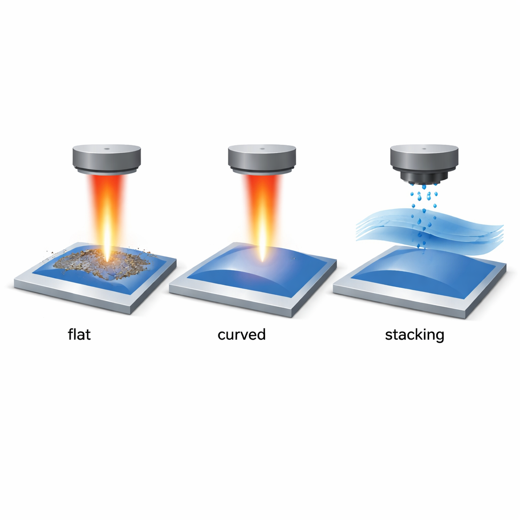
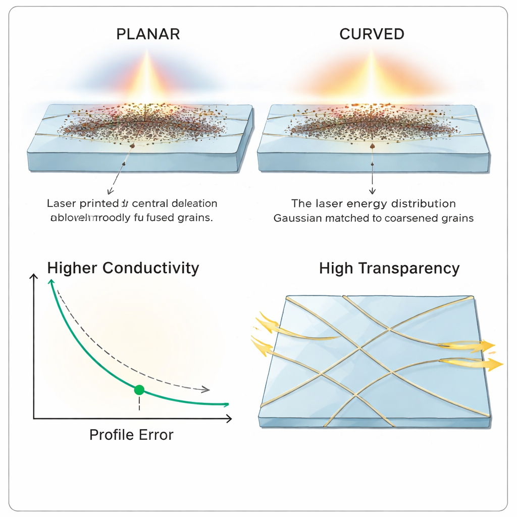
Industrial lasers almost always have a Gaussian profile: the light is most intense at the center of the spot and smoothly fades toward the edges. When such a beam scans across a flat, uniformly thick film of nanoparticles, the center gets too much energy and can ablate or vaporize, while the edges get too little and remain only partly fused. Engineers have tried to fix this by adding extra optics to flatten the beam profile, but these beam shapers are expensive, bulky, waste more than a third of the laser energy, and have limited lifetimes. As manufacturing moves toward flexible electronics and 3D-printed metals, these drawbacks become more serious.
Turning the Film Into a Gentle Hill
The authors propose a different tactic: keep the simple Gaussian laser, and instead tailor the thickness of the printed film so that it absorbs the right amount of energy everywhere. Using heat-transfer analysis, they derive how much energy each slice of material needs to sinter properly, and then calculate a matching thickness profile. The ideal shape turns out to be a smooth, Gaussian-like bump: thicker in the middle where the laser is strongest and thinner near the edges where it is weaker. When this “curved” track is scanned by a normal laser, the extra thickness at the center soaks up the excess energy, while the thinner edges make better use of the weaker light, leading to nearly uniform heating and grain growth across the entire width.
Printing Curved Tracks One Brick at a Time
Designing the ideal curve on paper is not enough; it must also be manufacturable. The team uses inkjet printing of nanoparticle inks to build the desired shape through controlled stacking of many narrow, nearly rectangular “unit” tracks. First, they solve a classic printing problem—the coffee-ring effect, where dried drops leave a thick rim and thin center—by using a two-solvent ink and heating the substrate so that internal flows in each droplet cancel out and produce flat-topped lines. By tuning temperature and droplet spacing, they can reliably print unit tracks of known width and height. Then, by overlapping these tracks with carefully chosen offsets, they assemble a smooth, Gaussian-like cross-section that closely matches the calculated ideal, with less than 2% deviation.
Sharper Circuits and Clearer Glass
To show what this approach can do, the researchers apply it to two types of circuits: transparent indium tin oxide (ITO) films on glass and copper (Cu) traces on curved surfaces. For ITO, the curved profiles yield up to 3.8 times higher electrical conductance than standard flat films made from the same amount of material, while also slightly increasing visible-light transmission by about 5%. The resulting conductive glass maintains its performance through repeated heating–cooling cycles and even shows better light transmission at oblique angles, thanks to its gentle, moth-eye-like surface. For copper, curved tracks reach conductivities around 1.6 times higher than flat, laser-processed counterparts, and they outperform both beam-shaped laser systems and conventional furnace sintering, all while using less energy and avoiding damage to heat-sensitive substrates like plastic films.
A Simple Idea with Broad Reach
In everyday terms, this work shows that you do not always need a fancier flashlight; sometimes you just need to carve the candle to match the light. By mathematically designing and inkjet-printing curved films that mirror the brightness profile of common lasers, the authors achieve more uniform sintering, higher conductivity, and better transparency without complex optics. This “curvature programmed” printing strategy could make it easier and cheaper to build high-performance flexible electronics, transparent heaters, antennae, and 3D-printed metal parts, using the same Gaussian lasers already widespread in industry.
Citation: Chen, X., Zhang, M., Zhu, J. et al. Curvature programmed inkjet printing enables adaptive deposition for Gaussian sintering lasers. Nat Commun 17, 2006 (2026). https://doi.org/10.1038/s41467-026-68613-y
Keywords: laser sintering, inkjet printed electronics, transparent conductive films, Gaussian beam shaping, flexible circuits