Clear Sky Science · en
A universal all-dry microfabrication method for sensitive electronic materials via an inorganic molecular lithographic mediator
Cleaning Up How We Make Tiny Electronics
Today’s smartphones, sensors, and flexible screens all rely on intricate patterns etched onto materials only atoms thick. Yet the liquids and chemicals used to sculpt these patterns can quietly damage the very materials they are meant to shape, especially the most delicate new semiconductors. This study introduces a dry, solvent-free way to pattern such fragile materials using a thin film of selenium, offering a cleaner path to future electronics.
Why Delicate Materials Need Gentler Tools
Modern chipmaking depends on lithography, where light or electrons draw patterns into special "resist" layers that are later washed in developers, removers, and cleaners. These steps involve water, strong bases, and organic solvents. That chemical bath is harsh for next-generation materials like perovskites, halides, and atomically thin sheets of black phosphorus or molybdenum disulfide. Liquids can react with them, roughen their surfaces, leave behind residue, or even change their composition, all of which weaken electrical performance. Protective coatings such as graphene can help, but they add complexity and do not fit smoothly into standard factory workflows.
A Dry Protective Film That Draws Its Own Patterns
The researchers instead turn to elemental selenium, an inorganic material that can be gently evaporated onto a wafer as a smooth, uniform film. In this form, selenium is built from small molecular rings and chains held together by weak forces. When a laser beam scans across the surface, the local heating breaks those weak bonds, and selenium in the illuminated regions simply sublimes away as vapor. This creates clean, sharp trenches and shapes directly in the selenium layer without any liquid development step. By tuning the laser color, power, and speed, the team achieves micrometer-scale lines and complex curves with nearly atomically flat exposed areas and no detectable selenium residue on the underlying substrate. 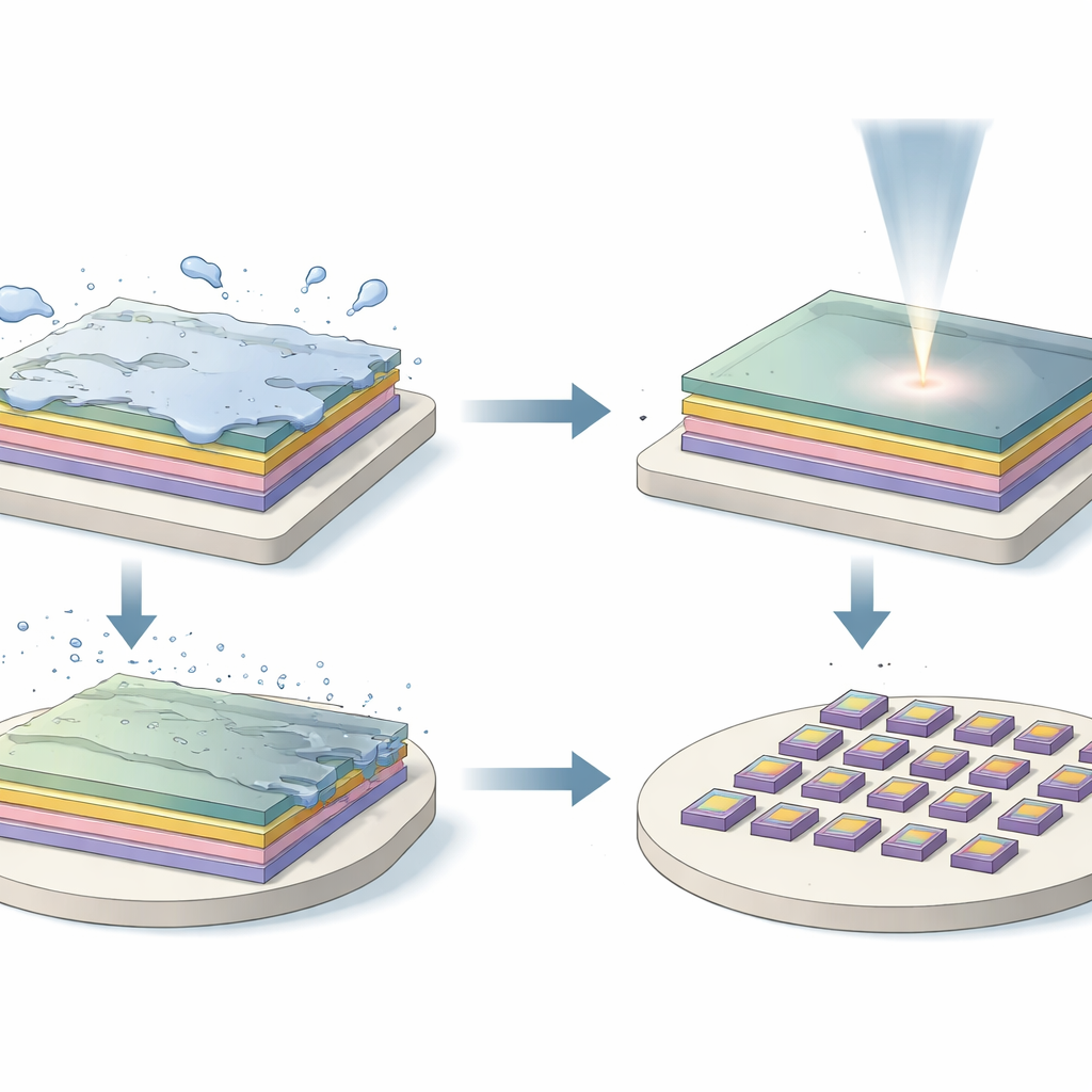
Peeling Instead of Washing
To turn these selenium patterns into functional devices, the team deposits metals or sensitive semiconductors over the patterned selenium and the exposed openings. Traditionally, a solvent would then dissolve the resist, lifting away unwanted regions. Here, the authors exploit a simple mechanical trick: they press a soft silicone layer (PDMS) onto the surface and peel it back. Because the bond between selenium and the wafer is intentionally weaker than the bond between the device material and the wafer, the PDMS lifts off the selenium and any material resting on it, while the desired patterns remain firmly attached to the substrate. Measurements show that the peeled surfaces are as smooth and clean as untouched wafer, and large-area arrays of halide crystals can be produced with uniform size and sharp edges, all without touching a drop of developer or remover. 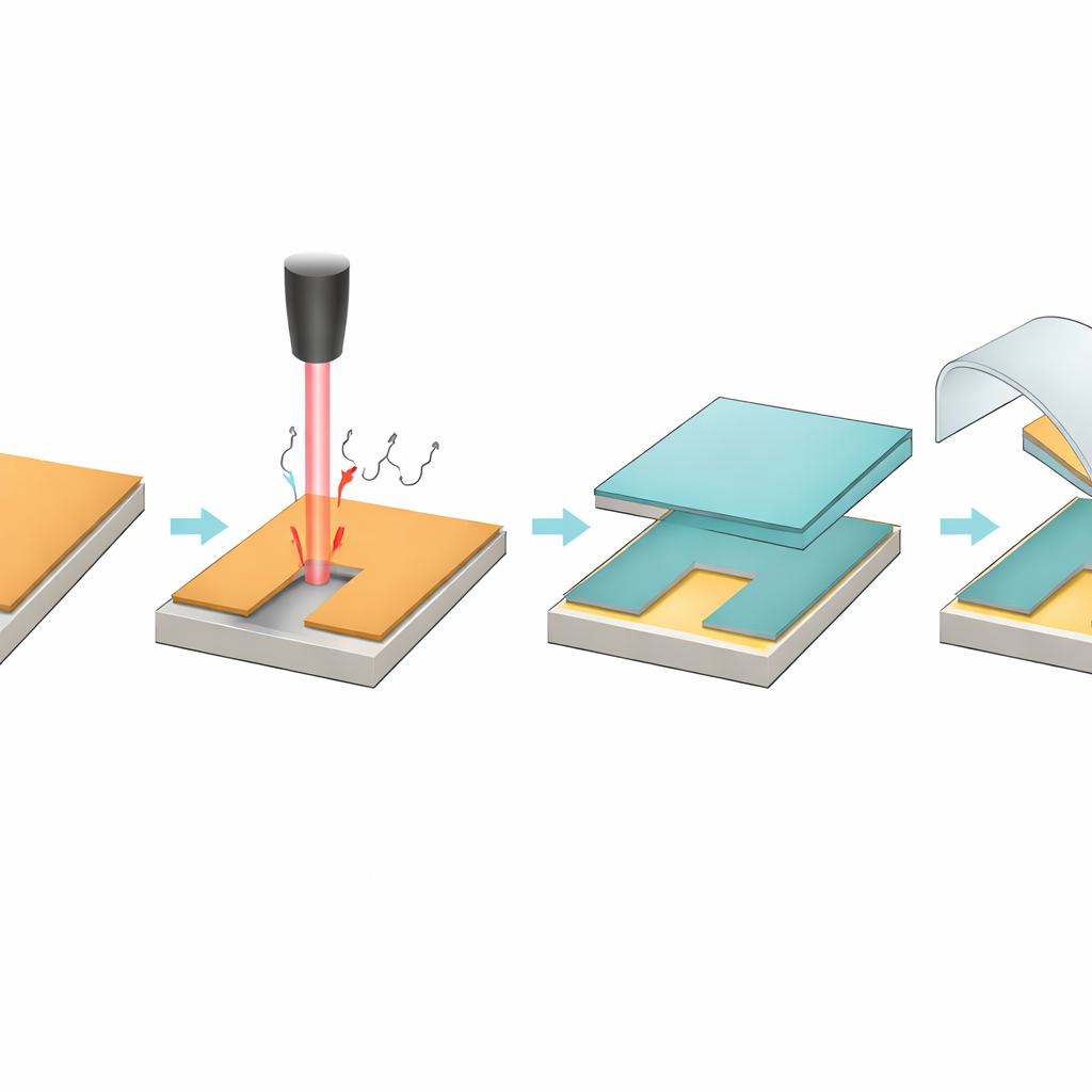
Keeping Fragile Crystals and 2D Sheets Intact
The true test is whether sensitive electronic materials survive this new process. The team compares selenium-based patterning with standard polymer resists for several fragile compounds, including lead halides, layered perovskites, lithium thiophosphates, magnesium phosphide sulfides, and black phosphorus. Under the dry selenium method, their shapes and surfaces remain essentially unchanged, and their characteristic light-emission and vibration signals stay stable—signs that their crystal structures are intact. Under conventional lithography, by contrast, surfaces become rougher, and the optical signals weaken or shift, revealing chemical damage and defects introduced by the solvents.
Better Transistors With Less Hidden Damage
Finally, the authors build real electronic devices to see how much this hidden damage matters in practice. Using selenium as a temporary shield, they fabricate field-effect transistors from black phosphorus and monolayer molybdenum disulfide on silicon wafers. The devices show clean, nearly ideal electrical behavior, with very high on/off current ratios and consistent performance across large arrays. When similar devices are made using standard organic resists, the transistor characteristics are noticeably poorer and less uniform. The improved performance indicates that carriers can move more freely because their atomically thin channels are not scarred or contaminated by chemical processing.
A Cleaner Road to Future Microchips
In everyday terms, this work replaces a messy wet-etching toolkit with a dry, peel-away stencil built from simple selenium molecules. By drawing patterns with light, then lifting off the protective layer mechanically instead of washing it away, the method shields fragile materials from harmful liquids while remaining compatible with existing chip manufacturing lines. As electronics increasingly rely on ultra-thin and chemically sensitive materials, this all-dry, selenium-mediated approach could help industry build faster, more reliable, and more energy-efficient devices without sacrificing the delicate structures that make them special.
Citation: Zeng, C., Xu, Y., Wei, X. et al. A universal all-dry microfabrication method for sensitive electronic materials via an inorganic molecular lithographic mediator. Nat Commun 17, 2098 (2026). https://doi.org/10.1038/s41467-026-68593-z
Keywords: dry lithography, selenium mediator, sensitive semiconductors, 2D materials, microfabrication