Clear Sky Science · en
Wafer-scale high-κ HfO2 dielectric films with sub-5-Å equivalent oxide thickness for 2D MoS2 transistors
Why Thinner Insulators Matter for Future Chips
Smartphones, data centers, and AI all rely on tiny electronic switches called transistors. To keep packing more of these switches into chips while cutting energy use, engineers must shrink not only the transistors themselves but also the insulating layers that control their behavior. This paper describes a way to make an extremely thin, high‑quality insulating film that still blocks electrical leakage, and to use it across full‑size wafers in cutting‑edge two‑dimensional (2D) transistor circuits.
A New Kind of Ultra-Thin Electrical Barrier
At the heart of every modern transistor is a "gate" that turns current on and off through a channel. Between them sits a thin insulating layer, or dielectric. For years, industry has used hafnium oxide (HfO2), a so‑called high‑κ material that allows strong control of the channel without needing a physically thick layer. But pushing this approach into the realm of a few atomic layers has been difficult: films often leak too much current or break down under electric stress. The authors introduce an improved growth method, called multiple oxidation atomic layer deposition (MOALD), that produces HfO2 films just 1.3 nanometers thick—only a few atoms—while keeping them dense and defect‑poor enough to function reliably. 
Cleaning Up Defects at the Atomic Scale
Conventional HfO2 growth in the lab usually uses a single oxidation step, which leaves behind many missing‑oxygen defects. These act like shortcuts for electrons, weakening the insulating power. In the MOALD approach, each growth cycle includes two oxidation steps, first with ozone and then with an oxygen plasma. Microscopy and spectroscopy show that this tandem treatment sharply reduces oxygen vacancies, yielding smoother, more continuous films even at 1.3 nanometers. Computer simulations back this up: when defects are plentiful, the electronic bandgap of the material shrinks and extra states appear inside the gap, which makes breakdown easier. When defects are minimized, the bandgap widens and leakage pathways are suppressed, restoring the strength of the dielectric.
Record-Thin Insulation with Low Leakage
The team measures these ultrathin films in simple metal–insulator–metal test structures. Despite their tiny physical thickness, the HfO2 layers behave like a much thinner layer of traditional silicon dioxide in terms of electrical control, achieving an equivalent oxide thickness of just 2.5 ångströms. That is below the aggressive targets laid out in international roadmaps for future logic devices. Crucially, leakage currents stay below one millionth of an ampere per square centimeter at operating voltages, and the films withstand electric fields above 22 megavolts per centimeter before breaking down. When compared with a wide range of experimental alternatives—such as exotic perovskites, molecular crystals, and other high‑κ oxides—these films combine very small effective thickness, low leakage, and strong breakdown behavior in a way that previous materials have struggled to match.
Bringing 2D Transistors and Circuits Closer to Reality
To show that the new dielectric is not just a laboratory curiosity, the authors integrate it with monolayer molybdenum disulfide (MoS2), a 2D semiconductor widely studied as a possible successor to silicon. They build two types of devices: gate‑first transistors, where the dielectric is grown before adding the MoS2, and gate‑last transistors, where it is deposited on top of an existing MoS2 layer using a thin antimony oxide “seed” layer. In both cases, devices switch cleanly, with on/off current ratios around one hundred million to one and near‑ideal subthreshold slopes close to the theoretical thermal limit. Short‑channel MoS2 transistors only 100 nanometers long deliver on‑state current densities up to 260 microamperes per micrometer at modest voltages, while gate leakage remains extremely low. 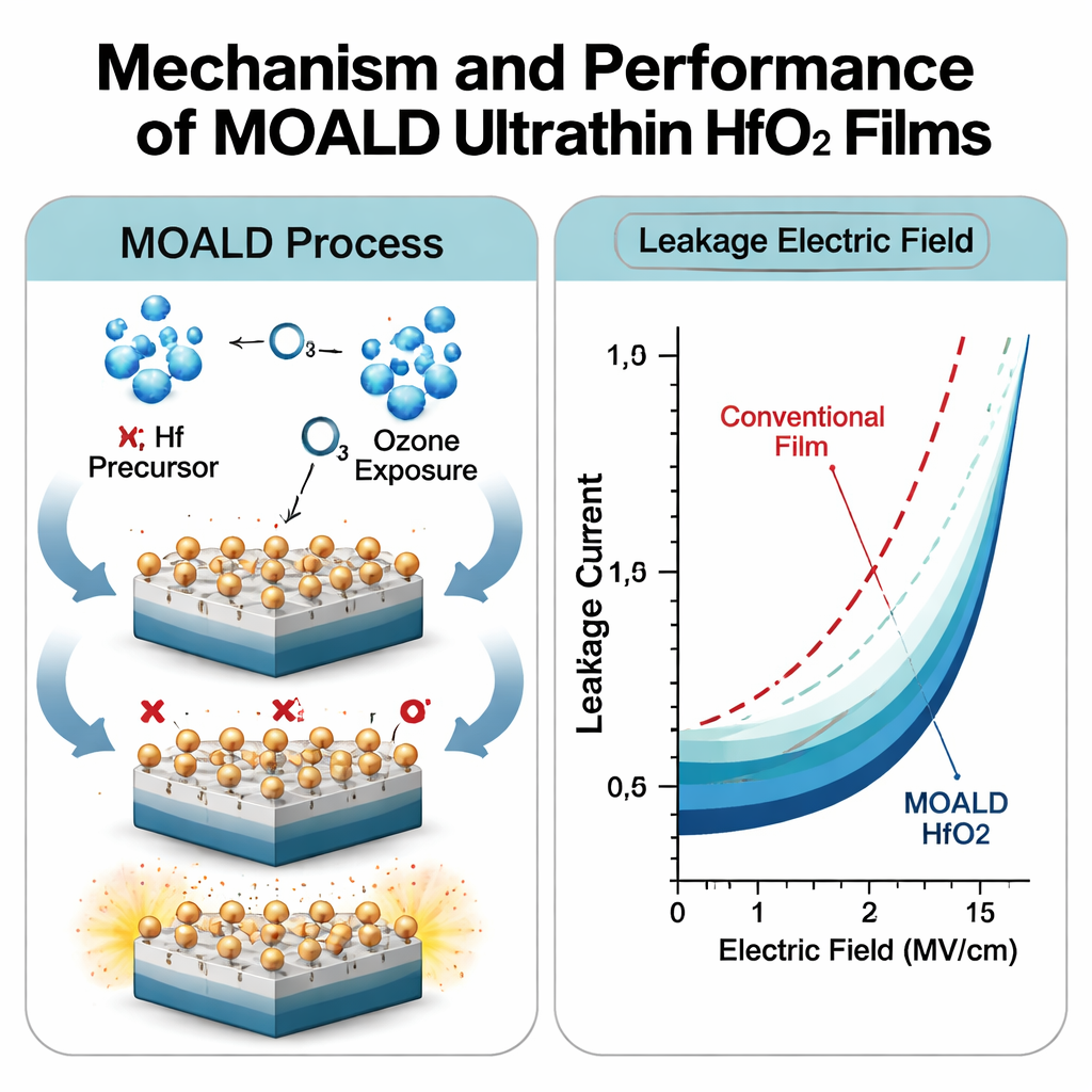
From Single Devices to Full Wafer Circuits
A key test for any new materials approach is whether it can be scaled to the large wafers used in industry. Here, the researchers grow their 1.3‑nanometer HfO2 layer uniformly across an 8‑inch silicon wafer at just 200 °C, a temperature compatible with standard chip manufacturing and with delicate 2D materials. On top of this, they fabricate wafer‑scale MoS2 logic circuits, including inverters, basic logic gates such as AND, NAND, and NOR, and five‑stage ring oscillators. These circuits operate correctly at unusually low supply voltages down to 0.1–0.2 volts, exhibit high gain, and consume tiny static power, illustrating how ultra‑thin, high‑quality dielectrics directly translate into low‑energy computation.
What This Means for Everyday Electronics
For non‑specialists, the takeaway is that the authors have built one of the thinnest practical electrical insulators ever used in a transistor, and they can manufacture it across full‑size wafers using industry‑friendly methods. By tightly controlling current with only a few atomic layers of material, these HfO2 films help 2D MoS2 transistors switch faster and waste far less energy. If such technologies can be further refined and integrated into commercial processes, they could prolong the trend of smaller, more efficient electronics, bringing future chips that are both more powerful and more energy‑frugal for applications ranging from mobile devices to large‑scale AI hardware.
Citation: Zhang, S., Zhang, T., Yu, H. et al. Wafer-scale high-κ HfO2 dielectric films with sub-5-Å equivalent oxide thickness for 2D MoS2 transistors. Nat Commun 17, 1888 (2026). https://doi.org/10.1038/s41467-026-68584-0
Keywords: high-k dielectrics, hafnium oxide, 2D MoS2 transistors, ultrathin gate insulators, low-power electronics