Clear Sky Science · en
Polar discontinuities, emergent conductivity, and critical twist-angle-dependent behaviour at wafer-bonded ferroelectric interfaces
Twisting Crystals to Make New Electronics
Electronic devices usually rely on what happens inside a material, not at its surface. This study shows that when two crystals are pressed and bonded together with a tiny twist between them, the interface where they meet can develop its own surprising behavior, including turning from an insulator into something that conducts electricity. Understanding and controlling this effect could open new ways to build ultra-thin, low-power electronic components without using traditional semiconductors.
Where Two Insulators Behave Like a Metal
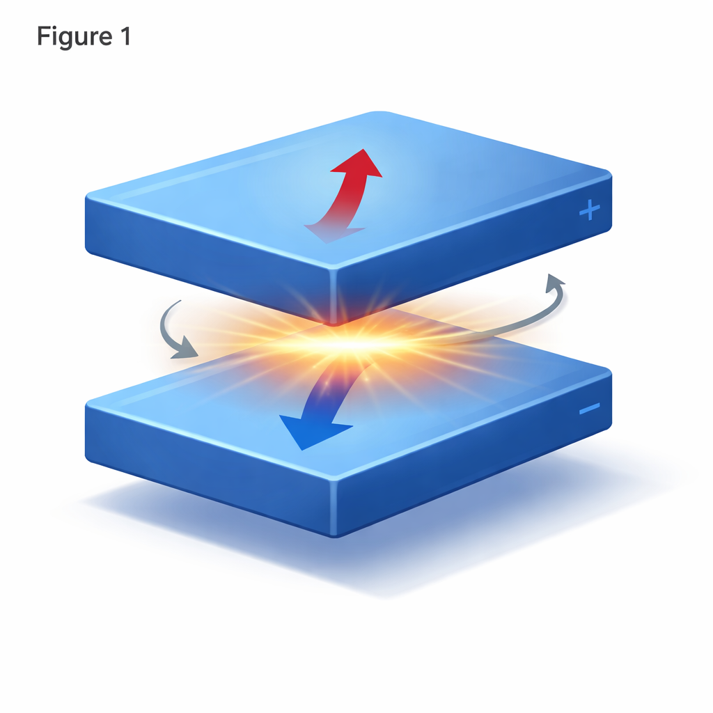
The researchers worked with lithium niobate, a well-known crystal used in optics and telecommunications. On its own, lithium niobate is a very good electrical insulator. However, it is also ferroelectric, meaning it carries a built-in electric polarization, like microscopic arrows pointing in a fixed direction inside the crystal. The team bonded two such crystals face to face so that these arrows pointed directly toward each other across the joining plane, creating what is called a “head-to-head” polar discontinuity. Theory suggests that such a configuration piles up electric charge at the interface. By using high-temperature thermocompression bonding—essentially pressing and heating the wafers together—they created atomically sharp, clean interfaces where this charge could accumulate.
A Hidden Sheet of Electricity at the Join
Careful imaging and electrical measurements showed that the bonded boundary between the crystals became a narrow, sheet-like conductor, even though the bulk of each crystal remained insulating. Using advanced electron microscopy, the team confirmed that the atomic lattice stayed continuous across the interface and that the crystal planes near the join were slightly compressed. Scanning probe techniques then mapped the local current flow and revealed that the conduction was confined to a region only a few nanometers thick, much like a two-dimensional electron gas in oxide electronics. Computer simulations based on quantum mechanics supported this picture: the abrupt change in polarization at the interface bends the electronic energy bands so that electronic states at the join cross the Fermi level, allowing charges to move freely along this plane.
Turning the Interface with a Twist
The story becomes even more intriguing when the two wafers are twisted relative to each other before bonding. For some twist angles—such as around 60 degrees—the interface still conducts well, and the original head-to-head polar arrangement is preserved. But at certain “critical” twist angles, including about 14, 21, and 74 degrees, the system reorganizes itself in a dramatic way. Instead of keeping the original configuration, the polarization near the interface flips direction over a layer roughly 15 micrometers thick, turning the boundary into a “tail-to-tail” configuration. This flip creates two new, conventional domain walls on either side of the join, which themselves become conducting paths, while the interface in the middle no longer behaves as the main conductor.
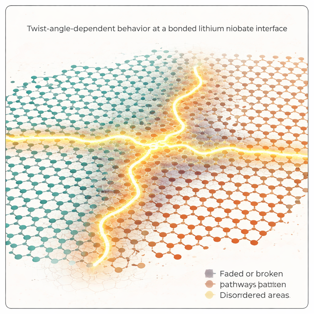
When Atomic Patterns Lose Their Regular Beat
Why should a tiny twist angle make such a big difference? The answer lies in how the two atomic lattices line up. At most angles, many lattice points from the two crystals coincide in a regular pattern, making it easier for charges to move along the interface and screen away the strong electric fields from the polar discontinuity. But at the special twist angles where the strange behavior appears, the shared lattice points become very sparse, and the pattern turns locally aperiodic—similar to what happens in quasicrystals. In such disordered arrangements, theory and past experiments in other systems show that electronic states can be suppressed, forming so-called pseudogaps and greatly reducing conductivity. The authors propose that something similar occurs here: the twist-induced aperiodicity shuts down the interfacial conduction, leaving the bound electric charge unscreened.
Electric Fields Strong Enough to Reshape the Crystal
With the interface no longer able to carry away charge, the resulting electric field becomes strong enough to flip the local polarization in the lithium niobate, even at the high temperatures used during bonding. This field-driven switching explains the observed inversion layer and the emergence of new conducting domain walls away from the initial join. The work shows that, by simply choosing the right twist angle between two ferroelectric wafers, one can toggle between different microscopic structures and conduction pathways. For a non-specialist, the main takeaway is that the boundary between two solids can be engineered, almost like a separate material, and that careful twisting offers a powerful new knob for designing future electronic and photonic devices.
Citation: Rogers, A., Holsgrove, K., Schäfer, N.A. et al. Polar discontinuities, emergent conductivity, and critical twist-angle-dependent behaviour at wafer-bonded ferroelectric interfaces. Nat Commun 17, 1842 (2026). https://doi.org/10.1038/s41467-026-68553-7
Keywords: twistronics, ferroelectrics, lithium niobate, oxide interfaces, two-dimensional conductivity